

Method for manufacturing a crystalline silicon layer
a manufacturing method and technology of crystalline silicon, applied in the direction of crystal growth process, chemical vapor deposition coating, coating, etc., can solve the problems of low temperature epitaxy on imperfect surfaces, high cost of solar cells, and devices with much lower efficiency than traditional solar cells, so as to reduce the amount of macroflatness, and reduce the amount of microroughness
- Summary
- Abstract
- Description
- Claims
- Application Information
AI Technical Summary
Problems solved by technology
Method used
Image

Examples
example 1
AIC on Bare Ceramic Substrate 1a (Comparative Example)
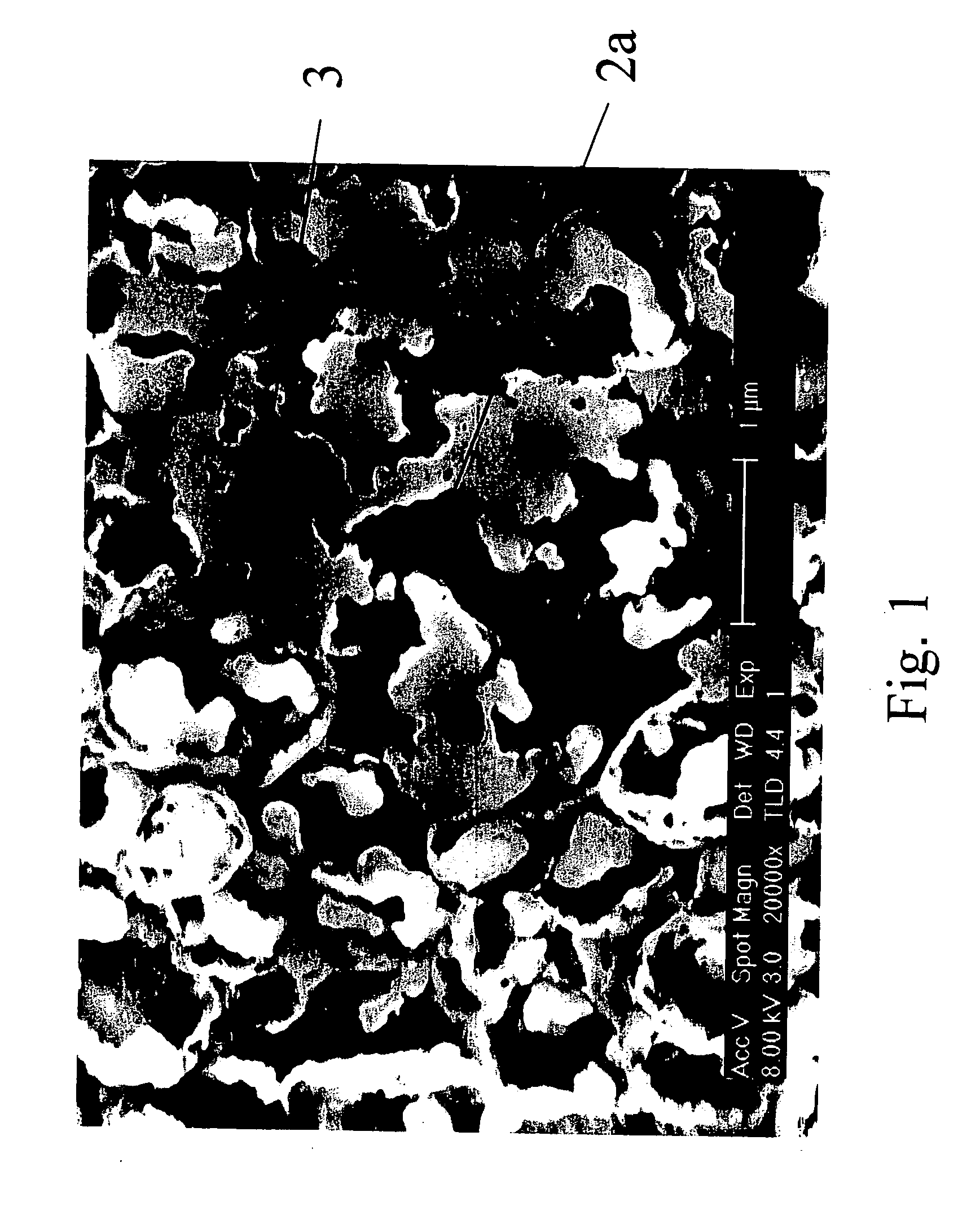
[0071] The morphology of a typical sample obtained with the procedure described above can be seen in the SEM picture in FIG. 1. The AIC seed layer 2a as such is not clearly visible in this picture. The reason is that the layer 2a is covered by numerous ‘islands’3, the secondary crystallites formed within the top layer during the AIC process. Close observation with SEM and TEM analysis reveals that the grain size in the AIC seed layer 2a is around 1-2 μm. This grain size is substantially lower than reported results on glass. There appears to be much more nucleation taking place when the AIC is done on a ceramic substrate 1a, both in the bottom layer (leading to a small grain size) and in the top layer (leading to a high density of islands).
example 2
Intermediate Layer Applied in Order to Reduce the Microroughness
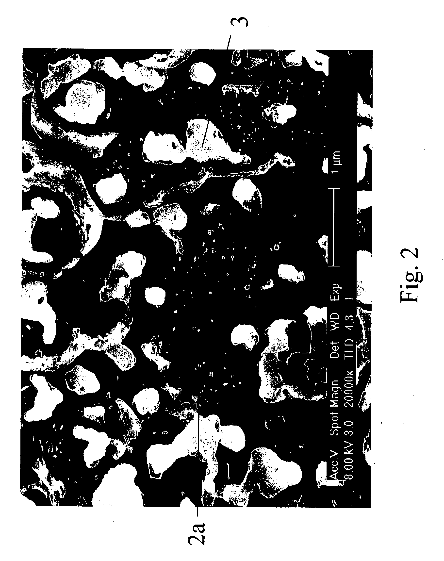
[0072] An intermediate silicon oxide layer was introduced between the substrate 1a and the AIC layers. Two different types of oxide were used. One type was a pyrolithic oxide (‘pyrox’) deposited by the decomposition of silane at atmospheric pressure and 400° C. The second type was a spin-on flowable oxide (FOx-23 from Dow Corning), cured at 400° C. Pyrox was densified at 950° C. and the spin-on flowable oxide at 900° C. before the deposition of the AIC stack. SEM pictures of these samples are shown in FIG. 2 and FIG. 3, respectively. The density of islands 3 decreased significantly compared to Example 1, by about a factor two for the intermediate pyrox layer (FIG. 2), and another factor 2 for the spin-on oxide layer (FIG. 3). The appearance of the latter samples is however completely different. Because there are much less islands 3 in the case of the spin-on oxide, the structure of the main AIC seeding layer 2a is clea...
example 3
Epitaxial Silicon Deposition
[0074] After removal of the metal layer obtained on top of the stack at the end of the MIC process, e.g. an Al layer in case of a AIC process, high temperature CVD was used to deposit an epitaxial layer on top of the seed layer 2a, an established technique common in the microelectronics processing. AIC seed layers 2a were prepared on spin-on flowable oxide 1b covering 5×5 cm2 alumina samples 1a following the procedure described above. The conditions were such that the AIC layers 2a covered the complete surface. No attempt was made at removing the islands 3 from the seed layer 2a. Si layers 2b were deposited on these samples in a commercial single-wafer epitaxial reactor (Epsilon ASM) with trichlorosilane diluted in H2, at atmospheric pressure and at a temperature of 1130° C. The deposition rate was 1.4 μm / min. In situ doping with B was done by adding diborane to the gas flow, so as to form double layers with a 0.5-3 μm thick p+ region (˜1019 cm-3) and a ...
PUM
| Property | Measurement | Unit |
|---|---|---|
| grain size | aaaaa | aaaaa |
| grain size | aaaaa | aaaaa |
| distance | aaaaa | aaaaa |
Abstract
Description
Claims
Application Information