Capacitor charging circuit with a soft-start function
- Summary
- Abstract
- Description
- Claims
- Application Information
AI Technical Summary
Benefits of technology
Problems solved by technology
Method used
Image

Examples
first embodiment
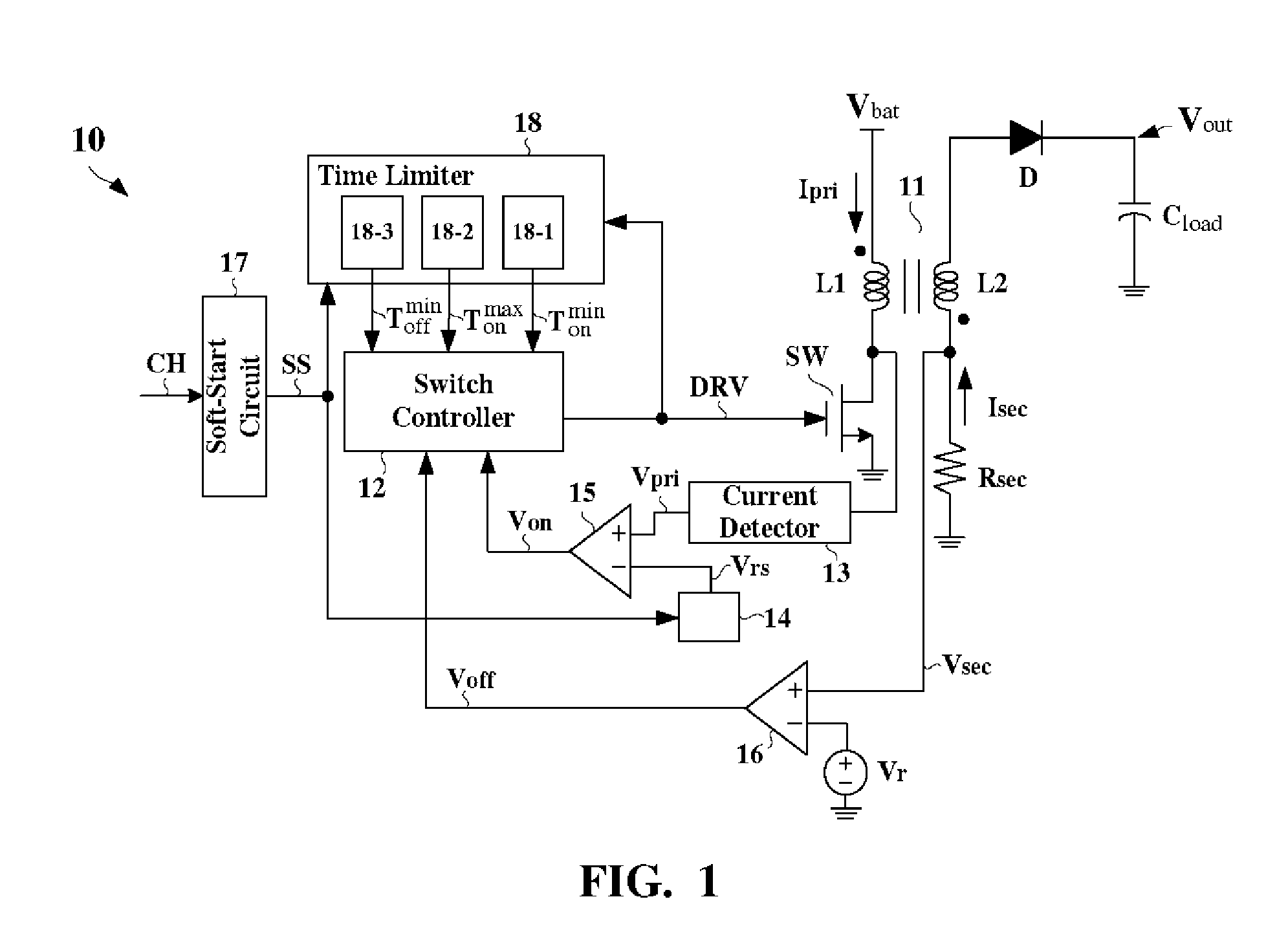
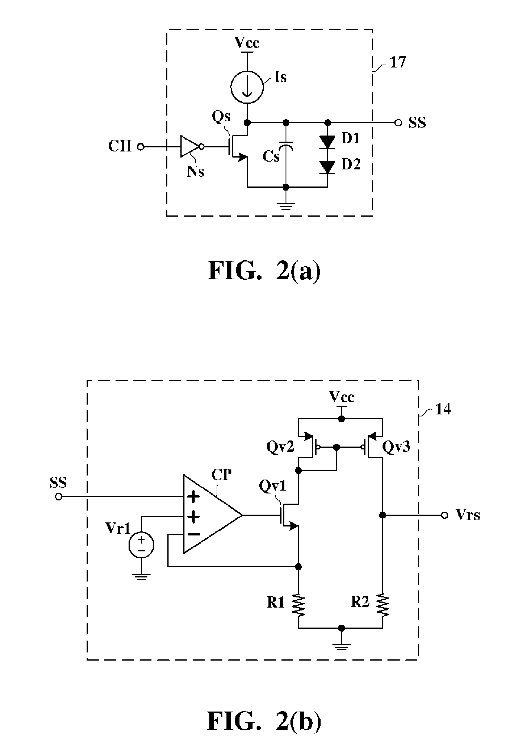
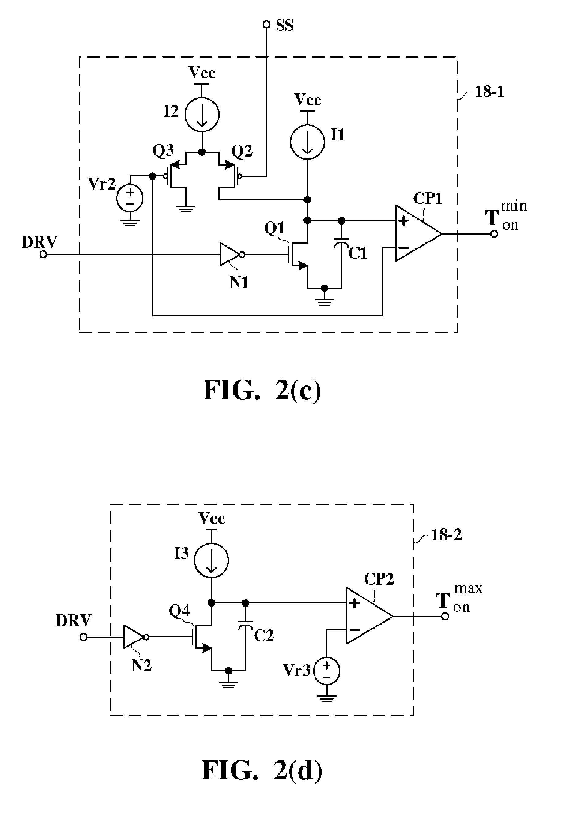
[0032]FIG. 1 is a circuit block diagram showing a capacitor charging circuit 10 according to the present invention. Referring to FIG. 1, under the ON / OFF switching operations of a power switch SW, a battery voltage Vbat is regulated to provide an output voltage for charging a capacitive load Cload. In one embodiment of the present invention, the power switch SW may be implemented by an NMOS transistor manufactured in a high voltage semiconductor process. A primary winding L1 and a secondary winding L2 are arranged to have opposite polarities, as indicated by black dots in FIG. 1, and therefore the transformer 11 belongs to a flyback type. When the power switch SW is at the ON state, the battery voltage Vbat supplies a primary winding current Ipri to store energy in the transformer 11. Meanwhile, a secondary winding current Isec is zero and the terminal voltage Vout across the capacitive load Cload remains unchanged. When the power switch SW is at the OFF state, the battery voltage V...
second embodiment
[0055]FIG. 7(c) is a detailed circuit diagram showing an example of the switch controller 12′ according to the present invention. As described above, since the ON-time ending signal Von′ is constrained at the LOW level before the minimum ON-time expires, the ON-time ending signal Von′ is equivalent in logic to the output signal of the AND logic gate A1 of FIG. 2(f). Likely, since the OFF-time ending signal Voff′ is constrained at the LOW level before the minimum OFF-time expires, the OFF-time ending signal Voff′ is equivalent in logic to the output signal of the AND logic gate A2 of FIG. 2(f). Therefore, in the switch controller 12′ of FIG. 7(c), the OR logic gate O1 has two input terminals coupled to the ON-time ending signal Von′ and the maximum ON-time limiting signal Tonmax, respectively. The SR latch LA has the reset input terminal R coupled to the output terminal of the OR logic gate O1, the set input terminal S coupled to the OFF-time ending signal Voff′, and the non-invertin...
PUM
 Abstract
Description
Claims
Application Information
 - R&D Engineer
- R&D Manager
- IP Professional
- Industry Leading Data Capabilities
- Powerful AI technology
- Patent DNA Extraction
Browse by: Latest US Patents, China's latest patents, Technical Efficacy Thesaurus, Application Domain, Technology Topic.
© 2024 PatSnap. All rights reserved.Legal|Privacy policy|Modern Slavery Act Transparency Statement|Sitemap