Reset in a system-on-chip circuit

a system-on-chip circuit and reset technology, applied in the direction of data conversion, transmission, automatic control, etc., can solve the problem of not having a mechanism to allow these types of reset signals

Active Publication Date: 2006-02-16
STMICROELECTRONICS (RES & DEV) LTD
View PDF8 Cites 17 Cited by
  • Summary
  • Abstract
  • Description
  • Claims
  • Application Information

AI Technical Summary

Benefits of technology

[0023] The integrated circuit can be used to advantage as part of a system-on-chip which has an input for receiving a data stream and an output for supplying a process da

Problems solved by technology

A problem arises when the system contains more than one clock environment. FIG. 2 illustrates a system on-chip 10 having an embedded CPU 2 and functional logic 14.
In this case, a problem arises with the use of soft reset signa

Method used


Image

  • Reset in a system-on-chip circuit
  • Reset in a system-on-chip circuit
  • Reset in a system-on-chip circuit

Examples


Embodiment Construction

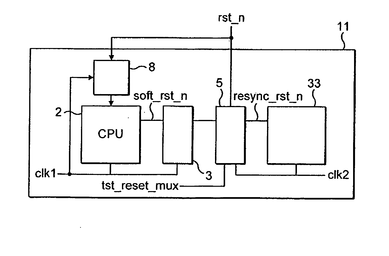
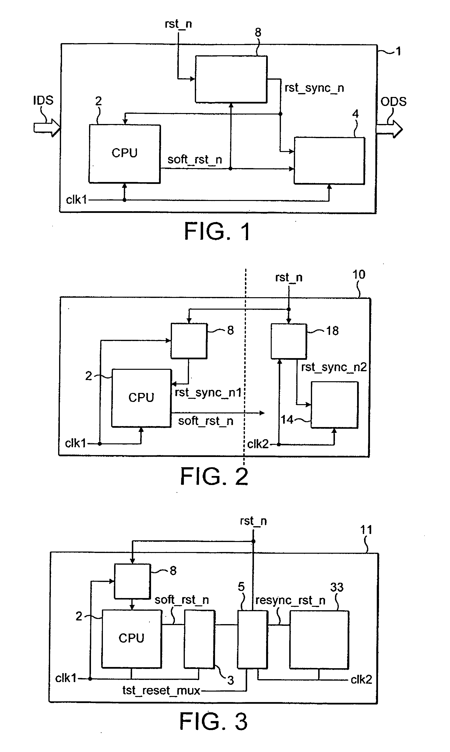
[0033]FIG. 3 illustrates schematically the environment of a system-on-chip 11 implementing an embodiment of the invention. The system on-chip 11 comprises an embedded CPU 2 operating in the first clock environment clk1 and which issues a soft reset signal soft_rst_n and supplies it to a soft reset hold circuit 3. Reference numeral 5 denotes a reset synchronizer which supplies a synchronization signal resync_rst_n to embedded functional logic 33 which operates in the second clock environment clk2. The soft reset hold circuit 3 receives the first clock clk1, while the synchronizer 5 receives the second clock clk2. A reset synchronizer 8 for a hard reset signal rst_n operates in the first clock environment as already described.

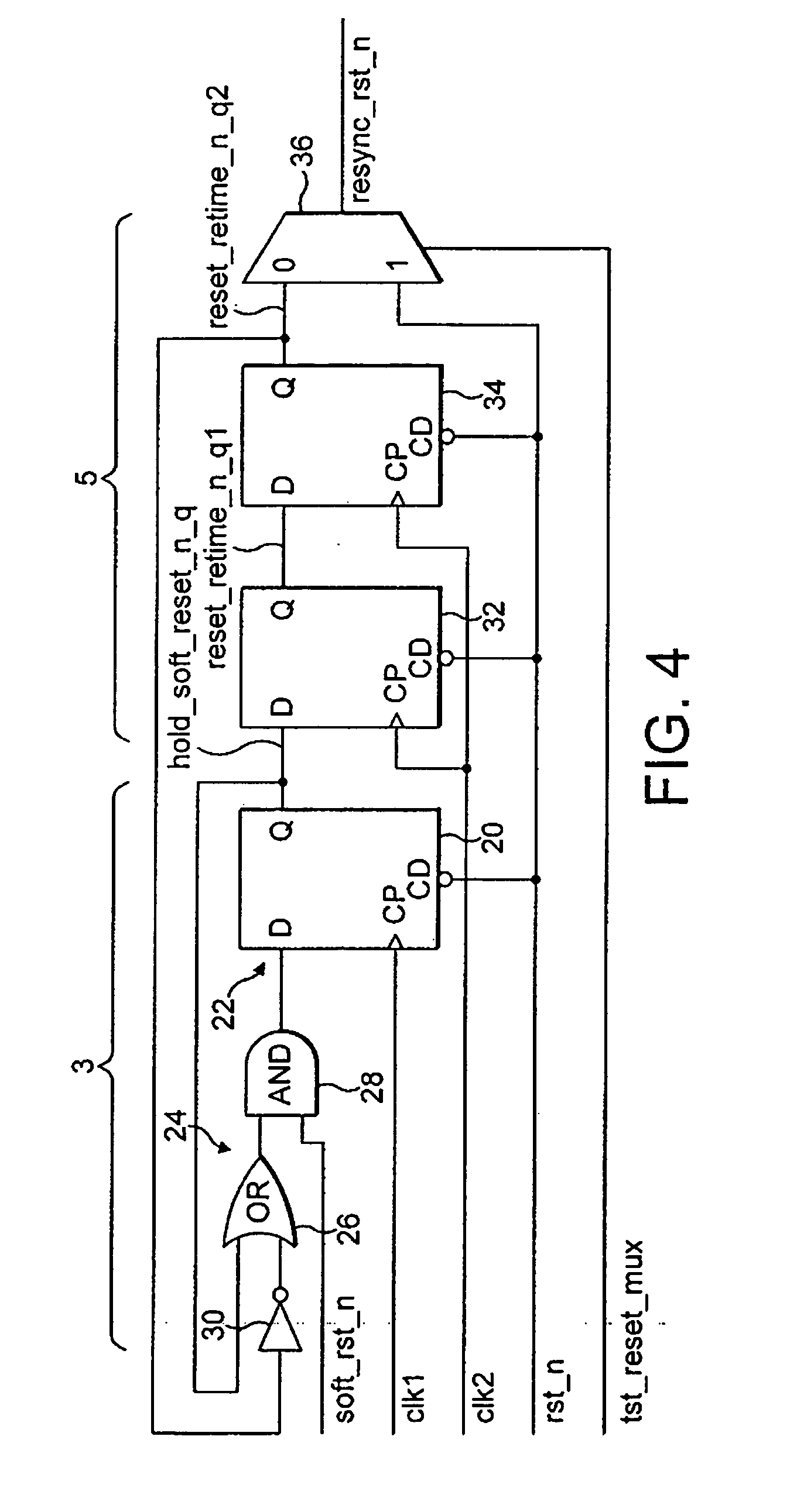
[0034]FIG. 4 illustrates the circuit structure according to one embodiment of the present invention. The soft reset hold circuit comprises a first flip-flop 20 which receives a clock signal from the first clock environment clk1. The flip-flop 20 has its CD input...


PUM


Abstract

An electronic device having first circuitry operating in a first clock environment and second circuitry operating in a second clock environment, the first circuitry being arranged to generate a soft reset signal for resetting the second circuitry, the integrated circuit further including: a soft reset hold circuit clocked in the first clock environment connected to receive the soft reset signal and to generate an output reset signal in an asserted state; and a synchronizer clocked in the second clock environment connected to receive the output reset signal and to generate a retimed reset signal in an asserted state after a predetermined period, wherein the retimed reset signal is fed back to the soft reset hold circuit to cause the output reset signal to adopt a deasserted state at the end of said predetermined period.

Description

BACKGROUND OF THE INVENTION [0001] 1. Field of the Invention [0002] This invention relates to reset in a system-on-chip circuit, in particular where there are two clock environments governing the operation of the circuitry on an integrated circuit. [0003] 2. Discussion of the Related Art [0004]FIG. 1 illustrates a system on-chip (SoC) in the form of an integrated circuit including a central processing unit (CPU) 2 and functional logic 4. The system-on-chip generally operates on an input data stream IDS (e.g. video, audio, etc) and generates a processed output data stream ODS. [0005] As in known in the art, the functional logic 4 within the system-on-chip integrated circuit may often need to be reset. By convention, reset signalling is performed using an active low signal and therefore given a name with a “_n” postfix to identify these signals as active low signals. Thus, rst_n=1 means that this is inactive, deasserted or not reset, while rst_n=0 means active, asserted or reset. [000...

Claims


Application Information

Patent Timeline
IPC IPC(8): G06F1/04
CPCG06F1/24
Inventor WARREN, ROBERTSMITH, DAVID
Owner STMICROELECTRONICS (RES & DEV) LTD
Why Eureka
Try Eureka