

Plasma processing apparatus and method
- Summary
- Abstract
- Description
- Claims
- Application Information
AI Technical Summary
Benefits of technology
Problems solved by technology
Method used
Image

Examples
embodiment 2
[0240] Next, an explanation will be given of the present invention.
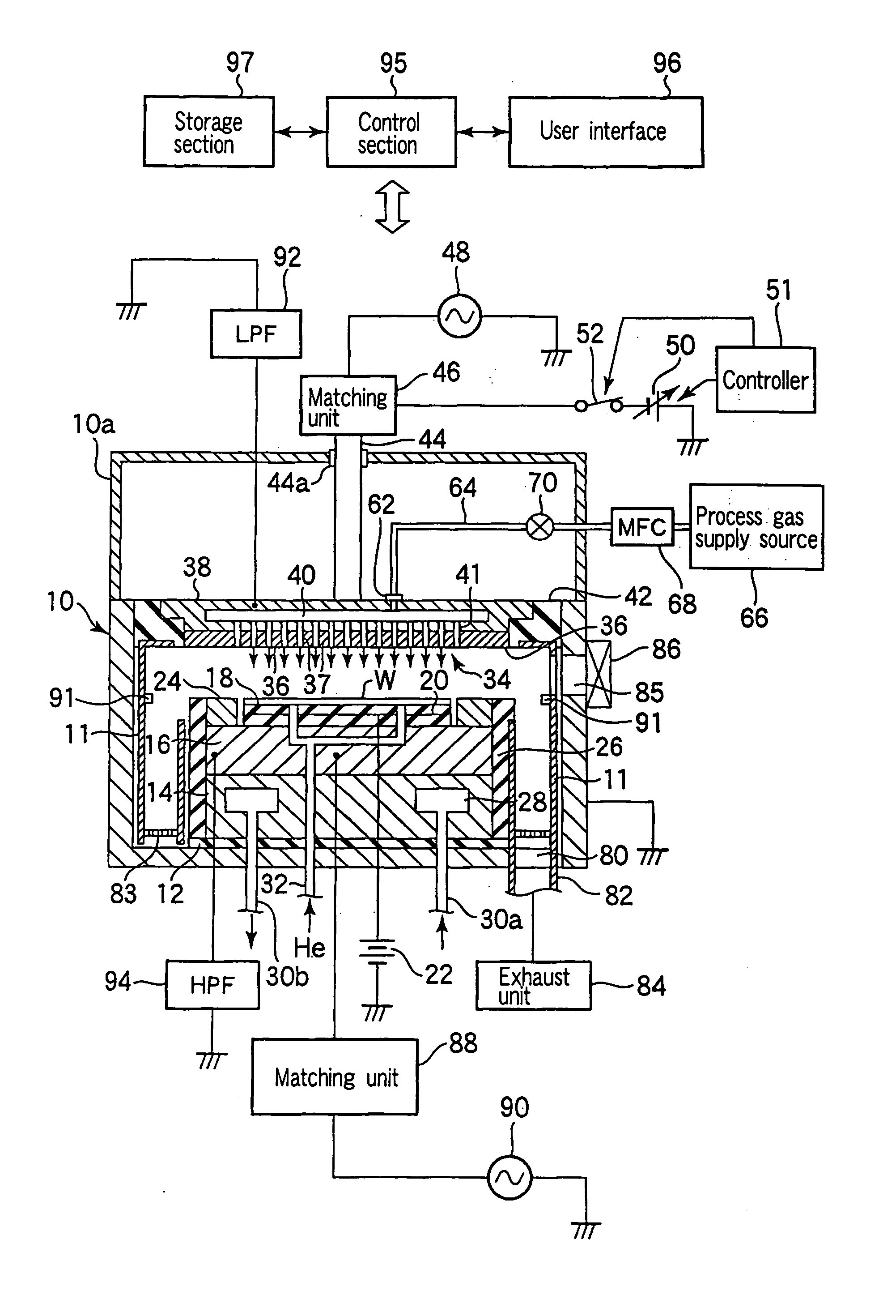
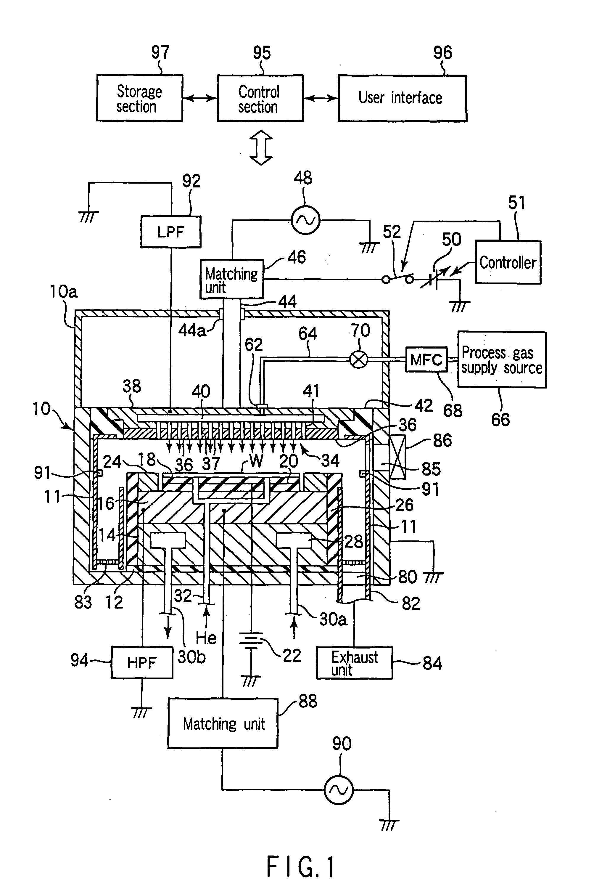
[0241]FIG. 34 is a sectional view schematically showing a plasma etching apparatus according to an embodiment 2 of the present invention. In FIG. 34, the constituent elements the same as those shown in FIG. 1 are denoted by the same reference symbols, and a repetitive description thereon will be omitted.
embodiment 1
[0242] In place of the upper electrode 34 of the embodiment 1, this embodiment includes an upper electrode 34′ having the following structure. Specifically, the upper electrode 34′ comprises an outer upper electrode 34a and an inner upper electrode 34b. The outer upper electrode 34a has a ring shape or doughnut shape and is disposed to face a susceptor 16 at a predetermined distance. The inner upper electrode 34b has a circular plate shape and is disposed radially inside the outer upper electrode 34a while being insulated therefrom. In terms of plasma generation, the outer upper electrode 34a mainly works for it, and the inner upper electrode 34b assists it.
[0243]FIG. 35 is an enlarged partial side view showing a main part of the plasma etching apparatus. As shown in FIG. 35, the outer upper electrode 34a is separated from the inner upper electrode 34b by an annular gap (slit) of, e.g., 0.25 to 2.0 mm, in which a dielectric body 72 made of, e.g., quartz is disposed. A ceramic body 7...
PUM
| Property | Measurement | Unit |
|---|---|---|
| Pressure | aaaaa | aaaaa |
| Power | aaaaa | aaaaa |
| Power | aaaaa | aaaaa |
Abstract
Description
Claims
Application Information