
Detection method for optimum position detection formula, alignment method, exposure method, device production method, device, and measurement and/or inspection apparatus

a detection method and optimum position technology, applied in the field of detection methods of optimum position detection formula, can solve problems such as overlay errors, deterioration of circuit formation characteristics, and lowering of overall yield

Inactive Publication Date: 2006-02-23
NIKON CORP
View PDF5 Cites 26 Cited by
  • Summary
  • Abstract
  • Description
  • Claims
  • Application Information

AI Technical Summary

Benefits of technology

[0022] An object of the present invention is to provide an alignment method enabling reduction of the effect on the throughput and nonlinear correction for the optimum shot arrangement for each wafer and an optimum position detection type detection method for the same.
[0024] Still another object of the present invention is to provide a method of production of a device using an exposure process with a good overlay accuracy and a high throughput to enable production of a high quality electronic device efficiently, that is, with a high productivity, and such a high quality device.

Problems solved by technology

Therefore, if the overlay accuracy between the layers is poor, the characteristics of the circuits formed deteriorate.
In the worst case, the semiconductor devices have to be discarded as defective and the overall yield is lowered.
However, such deviation of the position of a wafer in the exposure process, that is, the overlay error, sometimes includes nonlinear components.
In this case, usually there is error (stage grid error) between stage coordinate systems on exposure apparatuses.
This sometimes causes nonlinear overlay error.
This distortion of the wafer also causes nonlinear deviation, that is, overlay error.
Further, the polishing, heat expansion, etc. in the etching, CVD (chemical vapor deposition), CMP (chemical mechanical polishing), or other processing quite often causes distortion at the wafer.
Therefore, when exposing a layer after such a process, this distortion of the wafer causes nonlinear deviation, that is, overlay error.
This overlay error due to the prior processing also occurs even with overlay exposure in the same exposure apparatus with no stage grid error.
However, when the shot arrangement error is due to such stage grid error, distortion due to characteristics of the apparatuses, distortion due to processing, or other nonlinear wafer deformation, elimination by EGA is difficult.
However, in the first method, EGA has to be performed for close to all of the shots on each wafer, so the problem arises of deterioration of the throughput.
Further, in the second method, a single map correction file is selected for each process (exposure condition) for correction of the nonlinear components, so there is the problem that the nonlinear components of each wafer cannot be corrected at the same exposure sequence.

Method used


Image

  • Detection method for optimum position detection formula, alignment method, exposure method, device production method, device, and measurement and/or inspection apparatus
  • Detection method for optimum position detection formula, alignment method, exposure method, device production method, device, and measurement and/or inspection apparatus
  • Detection method for optimum position detection formula, alignment method, exposure method, device production method, device, and measurement and/or inspection apparatus

Examples


Embodiment Construction

[0067] An embodiment of the present invention will be explained in detail with reference to the drawings.

[0068] Exposure System

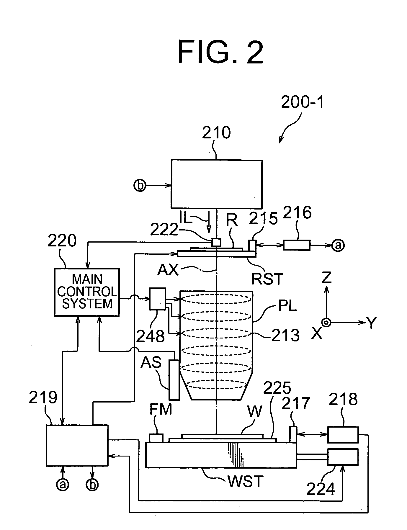
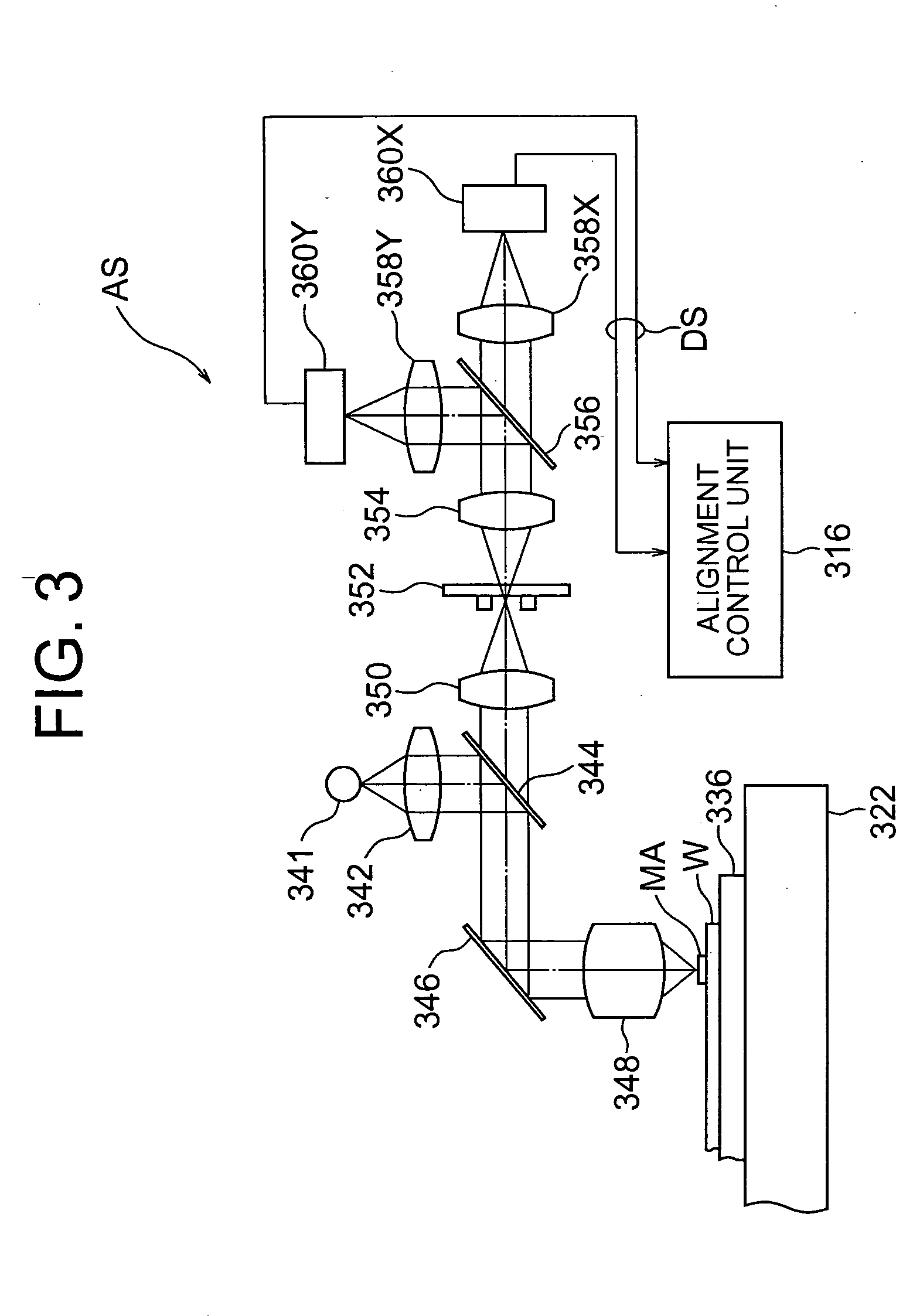
[0069] First, the overall configuration of an exposure system according to the present embodiment will be explained with reference to FIG. 1 to FIG. 3.

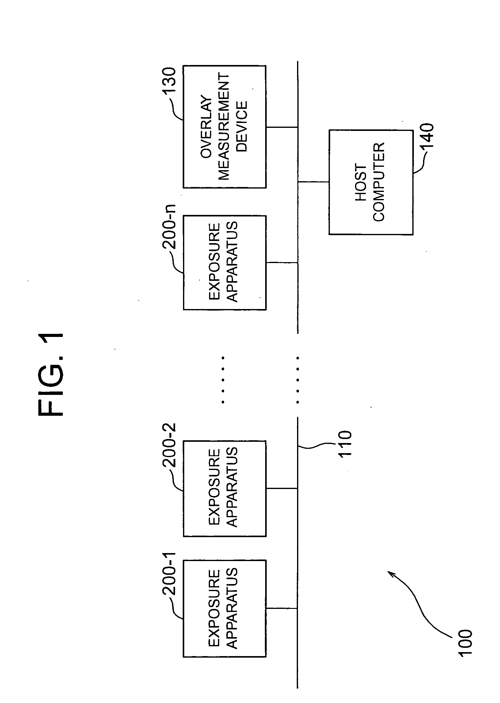
[0070]FIG. 1 is a view of the overall configuration of the exposure system 100 according to the present embodiment.

[0071] As shown in FIG. 1, the exposure system 100 has N number of exposure apparatuses 200-1 to 200-n, an overlay measurement device 130, and a host computer 140. These devices are connected by a LAN 110 so as to enable the transfer of data. Note that the LAN 110 may also have other processing devices, measurement devices, computers, etc. connected to it to enable transfer of data.

[0072] Each exposure apparatus 200-i (i=1 to n) (hereinafter simply referred to as an “exposure apparatus 200” in some cases) performs exposure processing on the wafers loaded in lot units (for example, 1 lot inclu...


PUM


Abstract

An alignment method enabling reduction of the effects on throughput and nonlinear correction for the optimum shot alignment for each wafer. According to the present invention, the nonlinear error is corrected by EGA calculation having higher order terms. One or more correction conditions (correction coefficients) are selected with reference EGA log data or overlay measurement data in advance for each process condition and registered in an exposure apparatus. At the time of lot processing of the exposure apparatus, the shot alignment of several sample shots is detected to detect the trend in nonlinear error and a single optimum correction coefficient is selected based on this from the registered plurality of correction coefficients. Further, after ordinary EGA, higher order EGA is performed using the selected correction coefficient to correct the nonlinear component and position each shot area.

Description

TECHNICAL FIELD [0001] The present invention relates to a detection method for an optimum position detection formula for aligning a photosensitive substrate suitable for use in a lithography process for production of for example a semiconductor device, liquid crystal display device, CCD, or other imaging device, a plasma display device, thin film magnetic head, or other electronic device (hereinafter simply referred to as an “electronic device”) and an alignment method for the same. Further, the present invention relates to an exposure method for exposure by alignment by this alignment method, a method of production of a device using this exposure method, and such a device. Furthermore, the present invention relates to a measurement and / or inspection apparatus. BACKGROUND ART [0002] In recent years, in the process of production of a semiconductor device or other electronic device, a step-and-repeat type, step-and-scan type, or other exposure apparatus, wafer prober, laser repair app...

Claims


Application Information

Patent Timeline
IPC IPC(8): G03F9/00G03C5/00G06K9/00G03F7/20H01L21/027
CPCG03F9/7003
Inventor OKITA, SHINICHI
Owner NIKON CORP
Learn More