

Electronic devices having a charge transport layer that has defined triplet energy level
a charge transport layer and electronic device technology, applied in the field of organic electronic devices, can solve the problems of low luminescence efficiency, low radiative rate of organic molecules, long lifetime, etc., and achieve the effect of reducing the number of transistors, and improving the efficiency of the charge transport layer
- Summary
- Abstract
- Description
- Claims
- Application Information
AI Technical Summary
Problems solved by technology
Method used
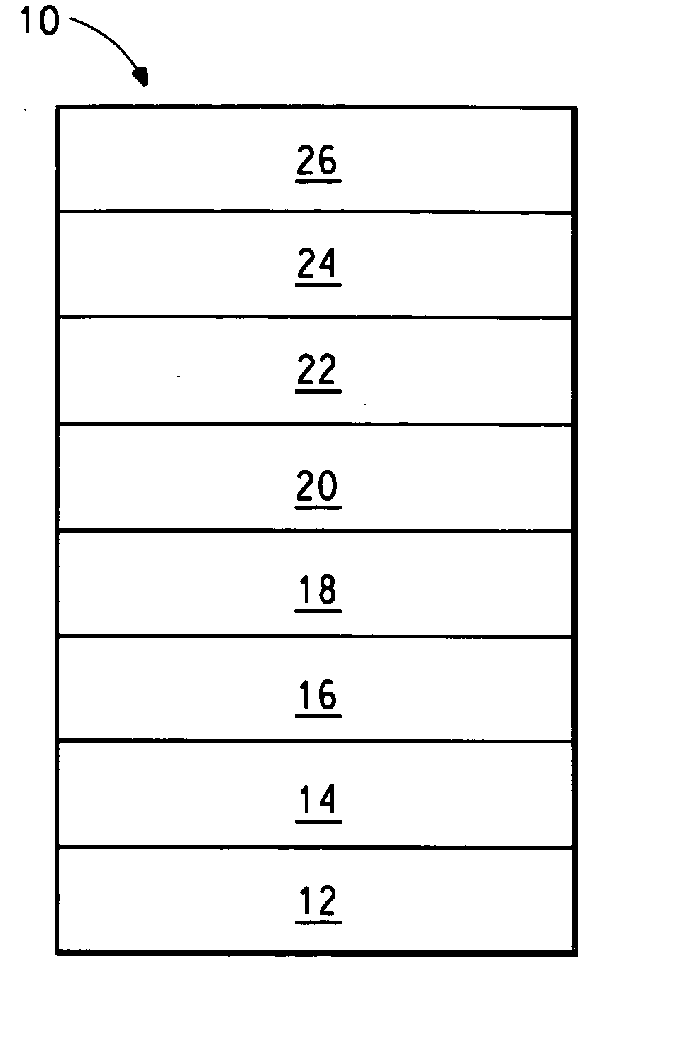
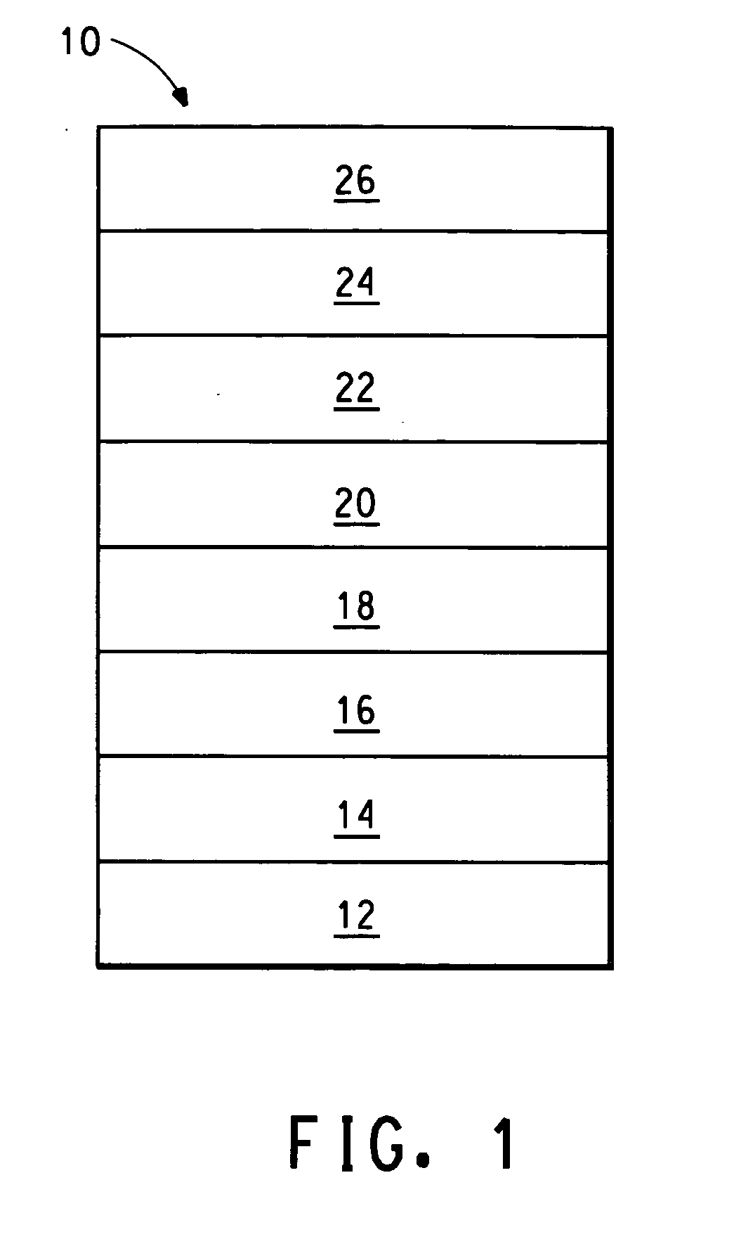
Image

Examples
example 1
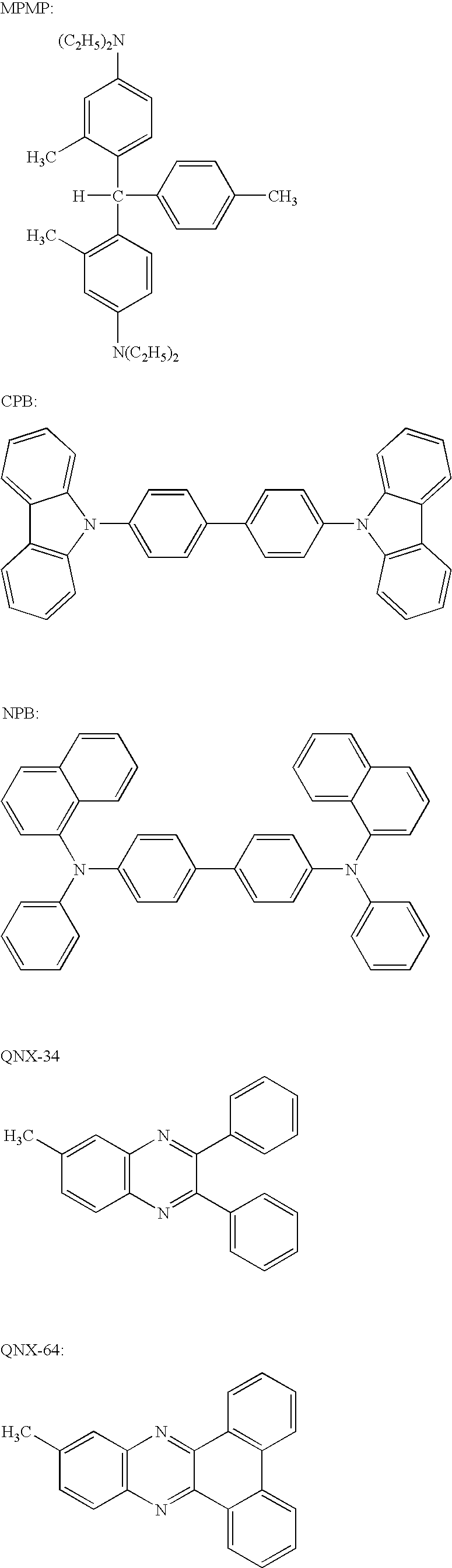
[0063] This example provides the triplet energy levels of different electron and hole transport materials as determined by pulse radiolysis / transient absorption method described above, and shows that there is incomplete correlation between triplet energy level and band gap size. Toluene was used as the solvent.
[0064] Table I shows the HOMO-LUMO gap (the bandgap) and the triplet energy levels of the different transport materials. Only the lower limit is listed for MPMP and only the upper limit is listed for QNX-64. The HOMO-LUMO gap of these materials are obtained by measuring the absorption edge of the material in toluene solvent.
TABLE ITriplet energy and HOMO-LUMO gap of a series ofelectron and hole transport materialsHOMOLUMO level,HOMO-LUMOTriplet energy,Moleculeslevel, eVeVgap, eVeVMPMP5.531.883.65>2.95NPB5.612.553.062.8CPB5.792.393.42.6QNX-346.53.243.262.73QNX-646.573.543.03
[0065] The molecular structures of these materials are as follows:
[0066] The data indicates that the...
example 2
[0067] This example illustrates the effect of charge transport material triplet energy level on device efficiency.
[0068] Thin film OLED devices including a hole transport layer (HT layer), electroluminescent layer (EL layer) and at least one electron transport layer (ET layer) were fabricated using the well known thermal evaporation technique. An Angstrom Engineering evaporator with cryopump was used to deposit the layers. The base vacuum for all of the thin film deposition was in the range of 10−6 torr. The deposition chamber was capable of continuously depositing a plurality of films while maintaining the vacuum.
[0069] Patterned indium tin oxide (ITO) coated glass substrates from Thin Film Devices, Inc. was used to form anode electrodes. These ITO substrates are based on Corning 1737 glass coated with 1400 Å ITO coating, with sheet resistance of 30 ohms / square and 80% light transmission. The patterned ITO substrates were then cleaned ultrasonically in aqueous detergent solution....
example 3
[0078] This example illustrates, via photoluminescence quenching experiments, that when the triplet energy of the charge transport material is lower than the exciton energy of the luminescent material, the luminescence intensity of the emitter material is quenched. The data in this example is consistent with the data in Example 2, which suggest that charge transport molecules having a higher triplet energy level make more efficient light emitting devices.
[0079] The effect of the triplet energy of the transport material on the luminescence efficiency of an emitter can be demonstrated via the photoluminescence quenching experiment. The luminescence quenching of an excited molecule can be described as
A*+Q→X (1)
where A* represents the luminescent excited state of the emitter, Q is the quencher (in this case the transport molecule under study), and X is the product of the quenching reaction. The rate constant of the luminescence quenching, kq, can be obtained by the well-known Stern...
PUM
 Abstract
Description
Claims
Application Information