Image pickup device
a pickup device and photoelectric technology, applied in the direction of photometry using electric radiation detectors, instruments, optical radiation measurement, etc., can solve the problems of insufficient durability of the device utilizing bcp, insufficient efficiency of light utilization, and large dimension and weight of the image pickup apparatus of such three-plate structure, etc., to achieve excellent durability and high photoelectric conversion efficiency
- Summary
- Abstract
- Description
- Claims
- Application Information
AI Technical Summary
Benefits of technology
Problems solved by technology
Method used
Image
Examples
example 1
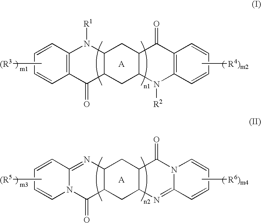
[0195] A washed ITO substrate was placed in an evaporation apparatus, and subjected to an evaporation of a quinacridone compound (S-9) of the invention with a thickness of 100 nm, and an evaporation thereon of Alq (aluminum quinoline) with a thickness of 50 nm to obtain an organic p-n laminated photoelectric conversion layer. Then a patterned mask (with an aperture of 2×2 mm) was placed on the organic film, and aluminum was evaporated with a thickness of 500 nm in the evaporation apparatus, then the device was sealed with a desiccant to obtain a photoelectric conversion device (device No. 101).
[0196] Also a device was prepared by replacing (S-9) with (S-8) (device No. 102).
example 2
[0197] After (S-9) was evaporated with a thickness of 100 nm as explained above, BAlq was evaporated with a thickness of 50 nm, then an electron transport material (E-1) was evaporated with a thickness of 70 nm, an aluminum electrode was evaporated as described above and the device was sealed to obtain a photoelectric conversion device (device No. 103).
example 3
[0198] After (S-9) was evaporated with a thickness of 100 nm as in Example 2, an electron transport material 24 was evaporated with a thickness of 100 nm, then an aluminum electrode was evaporated as described above and the device was sealed to obtain a photoelectric conversion device (device No. 104).
[0199] Similar devices were prepared by replacing (S-9) of the device No. 103 with (S-3), (S-6), (S-25), (S-8) and (S-10) (device Nos. 105, 106, 107, 108 and 109).
[0200] The devices were evaluated in the following manner.
[0201] A bias of 10 V was applied between the ITO at a minus side and the aluminum electrode at a plus side.
[0202] A wavelength dependence of an external quantum efficiency (IPCE) was evaluated by a solar cell evaluation apparatus, manufactured by Optel Inc. An obtained photoelectric conversion spectrum was used for a simulation to evaluate the spectral characteristics in a BGR device, and a level of the color reproducibility (spectral characteristics) was evaluat...
PUM
| Property | Measurement | Unit |
|---|---|---|
| half-peak width | aaaaa | aaaaa |
| wavelength | aaaaa | aaaaa |
| wavelength | aaaaa | aaaaa |
Abstract
Description
Claims
Application Information


