Optical semiconductor device and optical semiconductor in tegrated circuit

a technology of optical semiconductor and integrated circuit, which is applied in the direction of semiconductor lasers, instruments, optical elements, etc., can solve the problems of increasing power consumption, complicated device structure and control, and difficult to develop such a new semiconductor, and achieve the effect of suppressing the loss of refraction

Active Publication Date: 2006-03-09
NIPPON TELEGRAPH & TELEPHONE CORP
View PDF19 Cites 18 Cited by
  • Summary
  • Abstract
  • Description
  • Claims
  • Application Information

AI Technical Summary

Benefits of technology

[0045] Thus, the reflections on the interface surface between the first optical waveguide and the second optical waveguiding region and on the interface surface between the second optical waveguiding reg...

Problems solved by technology

However, as for the method of carrying out the temperature control of the semiconductor laser with the Peltier device, it has a problem of complicating the device structure and control, and increasing the power consumption.
As for the method of reducing the temperature dependence by the semiconductor-only configuration using the semiconductor material with the refractive index of smaller temperature dependence, no reports have been made about a new material that is put to practical use, and because of the crystal growth and device formation, it is very difficult to develop such a new semiconductor.
However, even if a simple fabrication method exists such as spin coating an organic material on the semiconductor substrate, in case for example of constructing distributed reflectors by alternately cascading the semiconductor and the organic materials to fabricate a first-order diffraction grating with good characteristics, it requires to place the semiconductor and organic materials alternately at about ¼ wavelength intervals, which presents a great degree of problem in the difficulty and reliability of the process.
However, it is difficult to form such an antireflection film at high accuracy when integrating the waveguide composed of different materials on a semiconductor substrate.
When splicing the semicondu...

Method used


Image

  • Optical semiconductor device and optical semiconductor in tegrated circuit
  • Optical semiconductor device and optical semiconductor in tegrated circuit
  • Optical semiconductor device and optical semiconductor in tegrated circuit

Examples


first embodiment

[0082] Several embodiments in accordance with the present invention will now be described with reference to the accompanying drawings. First, applications in a semiconductor laser will be described as a first embodiment with reference to several examples. This embodiment makes it possible to control the temperature dependence of the oscillation wavelength of a semiconductor laser by combining the semiconductor laser with materials having different temperature dependence of the refractive indices.

second embodiment

[0083] Second, applications in an integrated optical waveguide will be described as a second embodiment referring to several examples. This embodiment makes it possible, when integrating a semiconductor optical waveguide and an optical waveguide having refractive index and temperature dependence different from those of the semiconductor optical waveguide, to reduce the reflection on the interface surface between these optical waveguides. In addition, by integrating the semiconductor optical waveguide and the optical waveguide having the refractive index different from that of the semiconductor optical waveguide, the embodiment allows an implementation of an optical waveguide having new characteristics that cannot be achieved by semiconductor-only configurations.

third embodiment

[0084] Furthermore, as a third embodiment, by inclining the interface surface between a semiconductor optical waveguide and an optical waveguide having a different refractive index, with respect to the waveguide direction, the waveguide loss due to the reflection and refraction between these optical waveguides can be reduced. Also, by integrating the semiconductor optical waveguide and the optical waveguide having refractive index different from that of the semiconductor optical waveguide, the embodiment allows an implementation of an optical waveguide having new characteristics that cannot be achieved by semiconductor-only configurations.

(Applications in Semiconductor Laser)

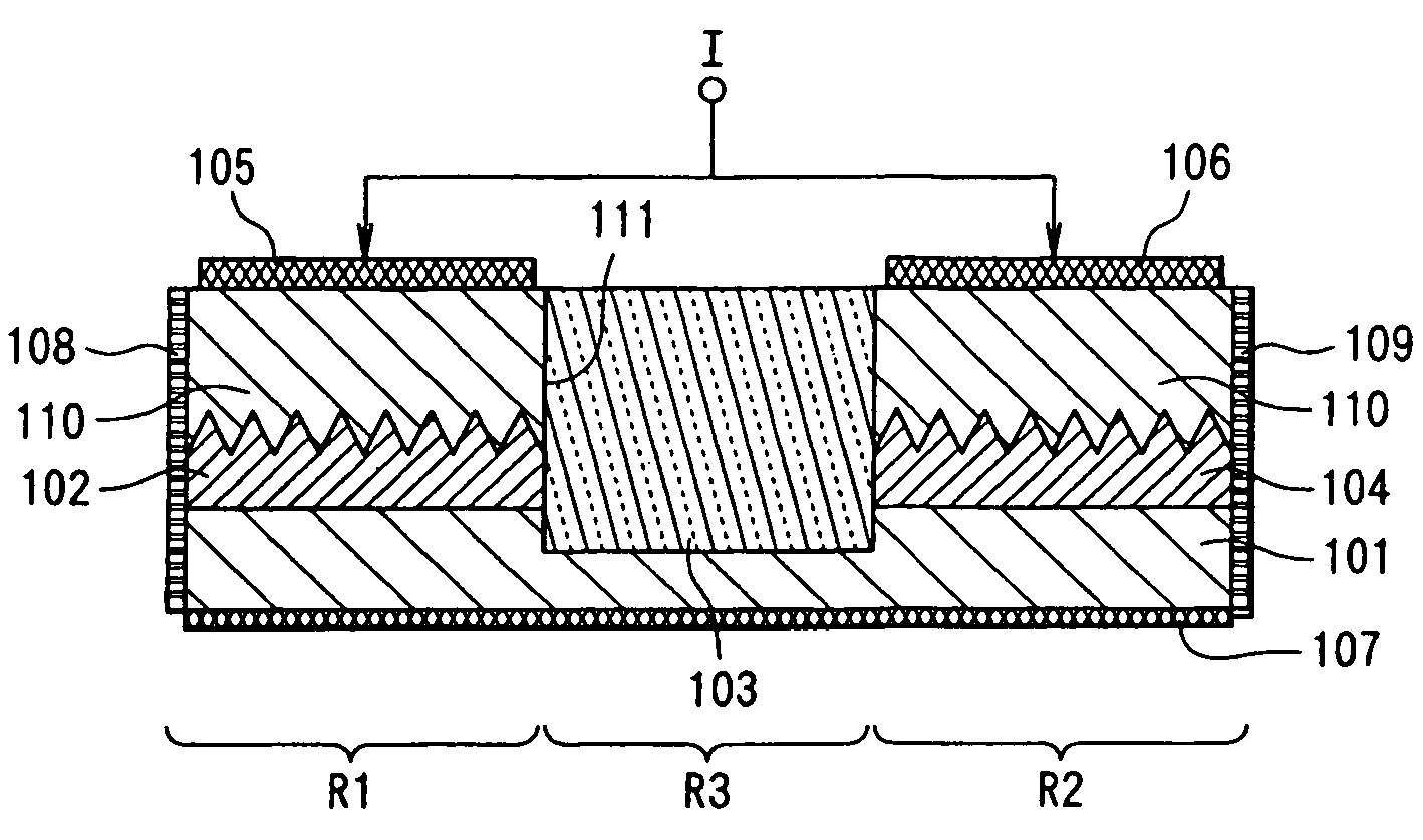
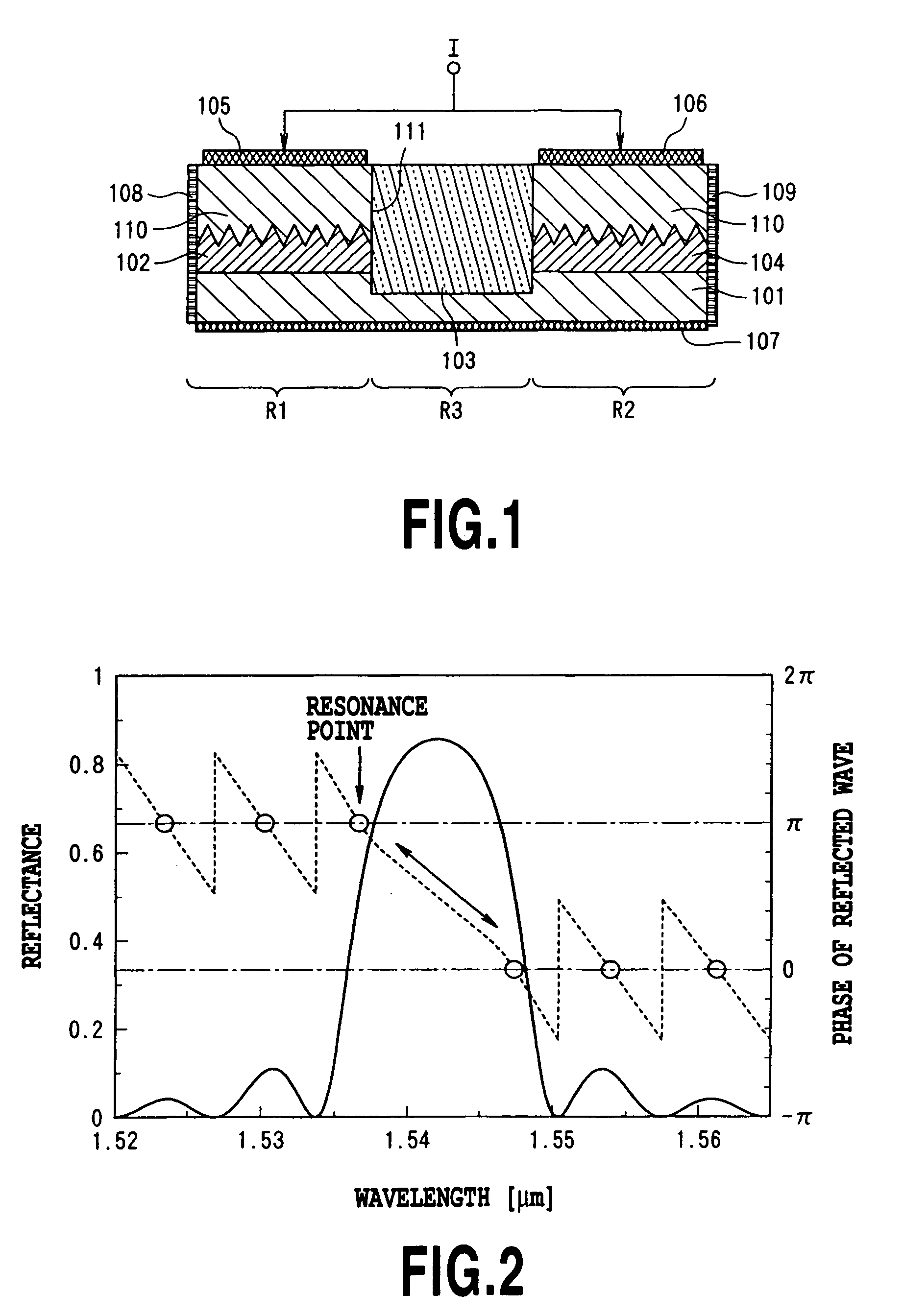
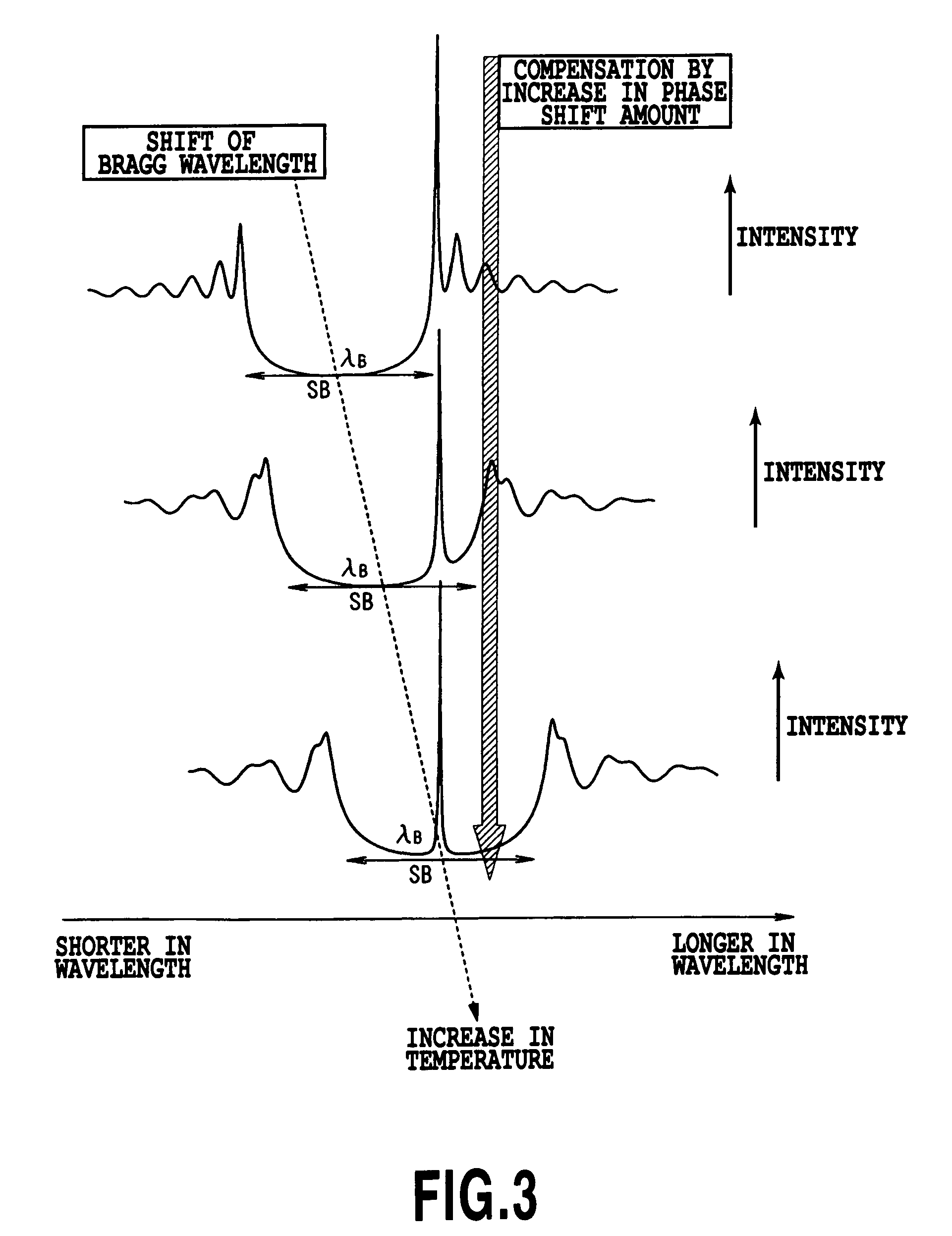
[0085] Semiconductor lasers of the first embodiment in accordance with the present invention will now be described with reference to the drawings. The first embodiment can provide semiconductor lasers capable of controlling the temperature dependence of the oscillation wavelength by combining materials differe...


PUM


Abstract

An optical semiconductor device and optical semiconductor integrated circuit are provided by combining, on a semiconductor substrate, materials having different refractive indices and different temperature dependence of the refractive indices. In particular, it becomes possible to control the temperature dependence of the oscillation wavelength with a propagating region having a material and/or structure whose temperature dependence of the refractive index is different from that of a gain region of the semiconductor laser. In addition, they can be configured to have a plurality of interfaces formed along the waveguide direction of the optical waveguide so that the light reflected off the first interface is weakened by the light reflected from the remaining interfaces. Also, they can be configured with the interfaces inclined to the propagating direction so that the waveguide loss due to the reflection and refraction between the optical waveguides whose refractive indices differ from each other can be reduced.

Description

FIELD OF THE INVENTION [0001] The present invention generally relates to an optical semiconductor device and optical semiconductor integrated circuit such as a semiconductor laser, optical waveguide, and other optical devices. The present invention particularly relates to an optical semiconductor device and optical semiconductor integrated circuit that are combined, on a semiconductor substrate, with materials which differ in the refractive indices and their temperature dependence. BACKGROUND ART [0002] The oscillation wavelength of a semiconductor laser varies depending on the ambient temperature and device temperature. For example, as described in K. Sakai, “1.5 μm range InGaAsP / InP distributed feedback lasers”, IEEE J. Quantum Electron, vol. QW-18, pp. 1272-1278, August 1982, the temperature dependence of the oscillation wavelength of a distributed feedback (DFB) laser is about 0.1 nm / K. This is because the refractive index (n) of a semiconductor has temperature dependence, and h...

Claims


Application Information

Patent Timeline
IPC IPC(8): H01S5/00H01S3/08G02B6/122G02B6/42H01S5/062H01S5/0625H01S5/068H01S5/10H01S5/12H01S5/125H01S5/22H01S5/227
CPCG02B6/12007H01S2301/173G02B6/131G02B6/136G02B6/4202H01S5/026H01S5/06206H01S5/06256H01S5/0654H01S5/068H01S5/101H01S5/1017H01S5/1025H01S5/1085H01S5/1215H01S5/1221H01S5/124H01S5/125H01S5/2205H01S5/227G02B6/122
Inventor NUNOYA, NOBUHIROSHIBATA, YASUOFUJIWARA, NAOKIKIKUCHI, NOBUHIROTOMORI, YUICHI
Owner NIPPON TELEGRAPH & TELEPHONE CORP
Why Eureka
Try Eureka