Organic electroluminescence device

a technology of electroluminescence device and organic el, which is applied in the direction of luminescnet screen, discharge tube luminescnet, natural mineral layered products, etc., can solve the problems of unstable electron transporting substance, chemical change of substance, and so as to improve the properties of organic el device, the effect of preventing the deterioration of electron transporting material due to hol

Inactive Publication Date: 2006-03-09
SANYO ELECTRIC CO LTD
View PDF5 Cites 21 Cited by
  • Summary
  • Abstract
  • Description
  • Claims
  • Application Information

AI Technical Summary

Benefits of technology

[0044] According to the second aspect of the present invention, since a hole which has invaded into an electron transporting layer can be stably trapped by a hole trapping material, deterioration of an electron transporting material due to a hole can be prevented. For this re

Problems solved by technology

In practical implementation of an organic EL device, a greatest problem is light emitting life property.
Herein, electrochemical deterioration of an organic substance means that a radical cation generated when an organic substance accepts a hole, or a radical a

Method used


Image

  • Organic electroluminescence device
  • Organic electroluminescence device
  • Organic electroluminescence device

Examples


example 1

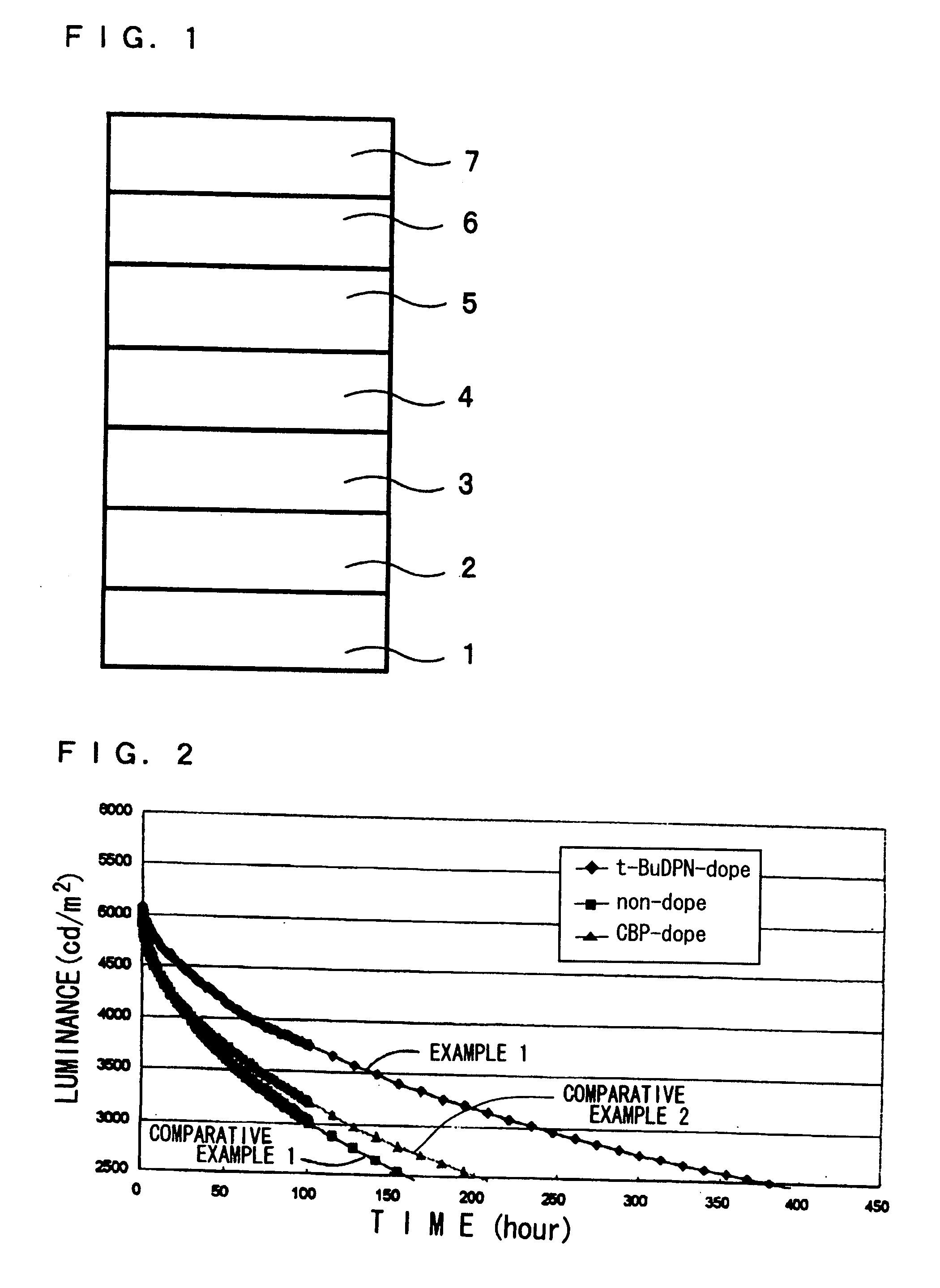
[0086] An organic EL device having a structure shown in FIG. 1 was prepared. In an organic EL device shown in FIG. 1, an anode buffer layer 2 is disposed on a hole injection electrode 1, a hole transporting layer 3 is disposed thereon, and a light emitting layer 4 is disposed thereon. A hole arresting layer 5 and an electron transporting layer 6 are disposed on a light emitting layer 4, and an electron injection electrode 7 is disposed on a electrode transporting layer 6. This organic EL device is prepared on a glass substrate. A hole injection electrode 1 is formed of ITO (indium tin oxide), and an anode buffer layer 2 (thickness 0.1 nm) using CFx is formed thereon. A hole transporting layer 3 (thickness 50 nm) containing 5% by weight of tBuDPN as an electron trapping material is formed thereon using NPB as a hole transporting material. A light emitting layer 4 (thickness 25 nm) consisting of CBP containing 6.5% by weight of Ir(ppy)3 is formed thereon. Ir(ppy)3 is tris(2-phenylpyri...

example 2

[0098] A white emitting organic EL device in which a light emitting layer was formed by laminating an orange emitting layer and a blue emitting layer, was prepared.

[0099]FIG. 10 is a cross-sectional view showing this white emitting organic EL device. As shown in FIG. 10, in this organic EL device, an anode buffer layer 12 is disposed on a hole injection electrode 11, and a hole transporting layer 13 is disposed thereon. An orange emitting layer 14 and a blue emitting layer 15 are disposed on a hole transporting layer 13 by lamination. An electron transporting layer 16 is disposed on these light emitting layers 14 and 15, and an electron injection electrode 17 is disposed on an electron transporting layer 16. This organic EL device is prepared on a glass substrate.

[0100] As in Example 1, a hole injection electrode 11 is formed of ITO, and an anode buffer layer 12 (thickness 1 nm) is formed of CFx.

[0101] A hole transporting layer 13 (thickness 110 nm) is formed of NPB containing 5%...

example 3

[0133] An organic EL device having a structure shown in FIG. 13 was prepared. In the organic EL device shown in FIG. 13, an anode buffer layer 22 is disposed on a hole injection electrode 21, a hole transporting layer 23 is disposed thereon, and a light emitting layer 24 is disposed thereon. An electron transporting layer 25 is disposed on a light emitting layer 24, and an electron injection electrode 26 is disposed on an electron transporting layer 25. This organic EL device is prepared on a glass substrate. A hole injection electrode 21 is formed of ITO (indium tin oxide), and an anode buffer layer 22 (thickness 0.1 nm) is formed thereon. A hole transporting layer 23 (thickness 50 nm) using NPB as a hole transporting material is formed thereon. A light emitting layer 24 (thickness 30 nm) consisting of Alq is formed thereon.

[0134] An electron transporting layer 25 (thickness 20 nm) uses BCP as an electron transporting material, and contains 5% by weight of m-MTDATA as a hole trapp...


PUM

PropertyMeasurementUnit
Percent by massaaaaaaaaaa
Poweraaaaaaaaaa
Poweraaaaaaaaaa

Abstract

An organic electroluminescent device in which a light emitting layer is disposed between a hole injection electrode and an electron injection electrode, and a hole transporting layer is disposed between a hole injection electrode and a light emitting layer, wherein the hole transporting layer contains an electron trapping material exhibiting a reversible cathode reduction process in cyclic voltammetry measurement and having a reduction potential smaller than that of a hole transporting material contained in the hole transporting layer, or wherein the electron transporting layer contains a hole trapping material exhibiting a reversible anode reduction process in cyclic voltammetry measurement and having an oxidation potential smaller than that of an electron transporting material contained in the electron transporting layer.

Description

[0001] The priority Japanese Patent Application Numbers 2004-89208, 2004-89210 and 2004-374056 upon which this patent application is based is hereby incorporated by reference. BACKGROUND OF THE INVENTION [0002] 1. Field of the Invention [0003] The present invention relates to an organic electroluminescence device, more particularly, an organic electroluminescence device excellent in light emitting life property. [0004] 2. Description of the Related Art [0005] An organic electroluminescence device (organic EL device) is being actively developed from a viewpoint of application to display and illumination. A principle of driving an organic EL device is as follows. That is, a hole and an electron are injected from a hole injection electrode and an electron injection electrode, respectively, they are transported into an organic thin film, and recombined in a light emitting layer, thereby, the excited state is generated, and light emission is obtained from this excited state. [0006] In pr...

Claims


Application Information

Patent Timeline
IPC IPC(8): H05B33/12H01L51/00H01L51/50H05B33/14H05B33/22
CPCH01L51/0054H01L51/0058H01L51/0059Y10T428/24942H01L51/0081H01L51/0085H01L51/5052H01L51/0072H10K85/622H10K85/631H10K85/626H10K85/324H10K85/342H10K85/6572H10K50/155H10K50/165C09K11/06H05B33/22
Inventor OKUMOTO, KENJIKANNO, HIROSHI
Owner SANYO ELECTRIC CO LTD
Why Eureka
Try Eureka