Large-grain p-doped polysilicon films for use in thin film transistors

a technology of polysilicon and thin film, which is applied in the direction of semiconductor devices, electrical equipment, basic electric elements, etc., can solve the problems of degrading device performance and reducing carrier mobility

Active Publication Date: 2006-03-09
SANDISK TECH LLC
View PDF12 Cites 26 Cited by
  • Summary
  • Abstract
  • Description
  • Claims
  • Application Information

AI Technical Summary

Problems solved by technology

However, when the channel region of a transistor is formed in a polysilicon layer, grain boundaries in the polys

Method used


Image

  • Large-grain p-doped polysilicon films for use in thin film transistors
  • Large-grain p-doped polysilicon films for use in thin film transistors
  • Large-grain p-doped polysilicon films for use in thin film transistors

Examples


example

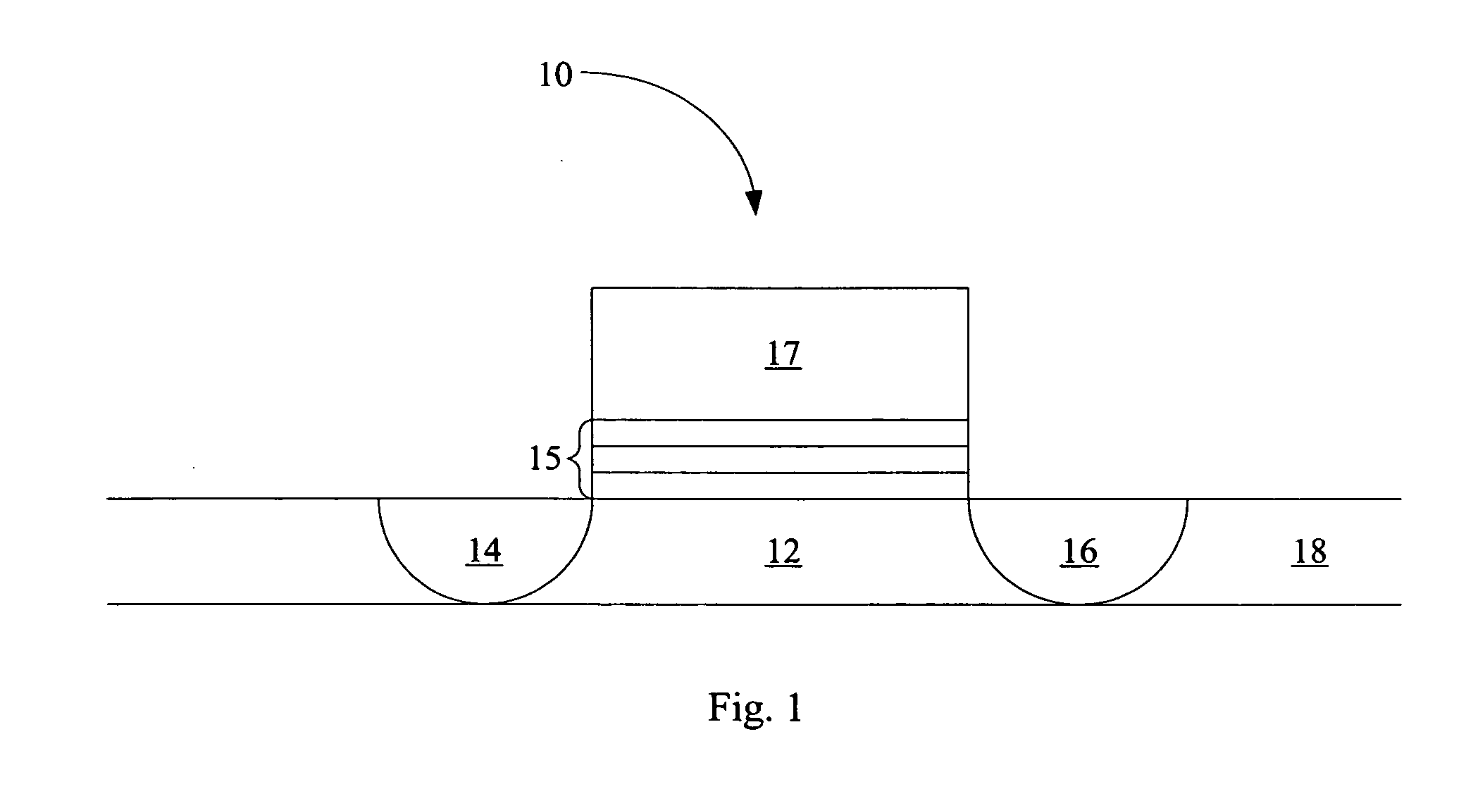
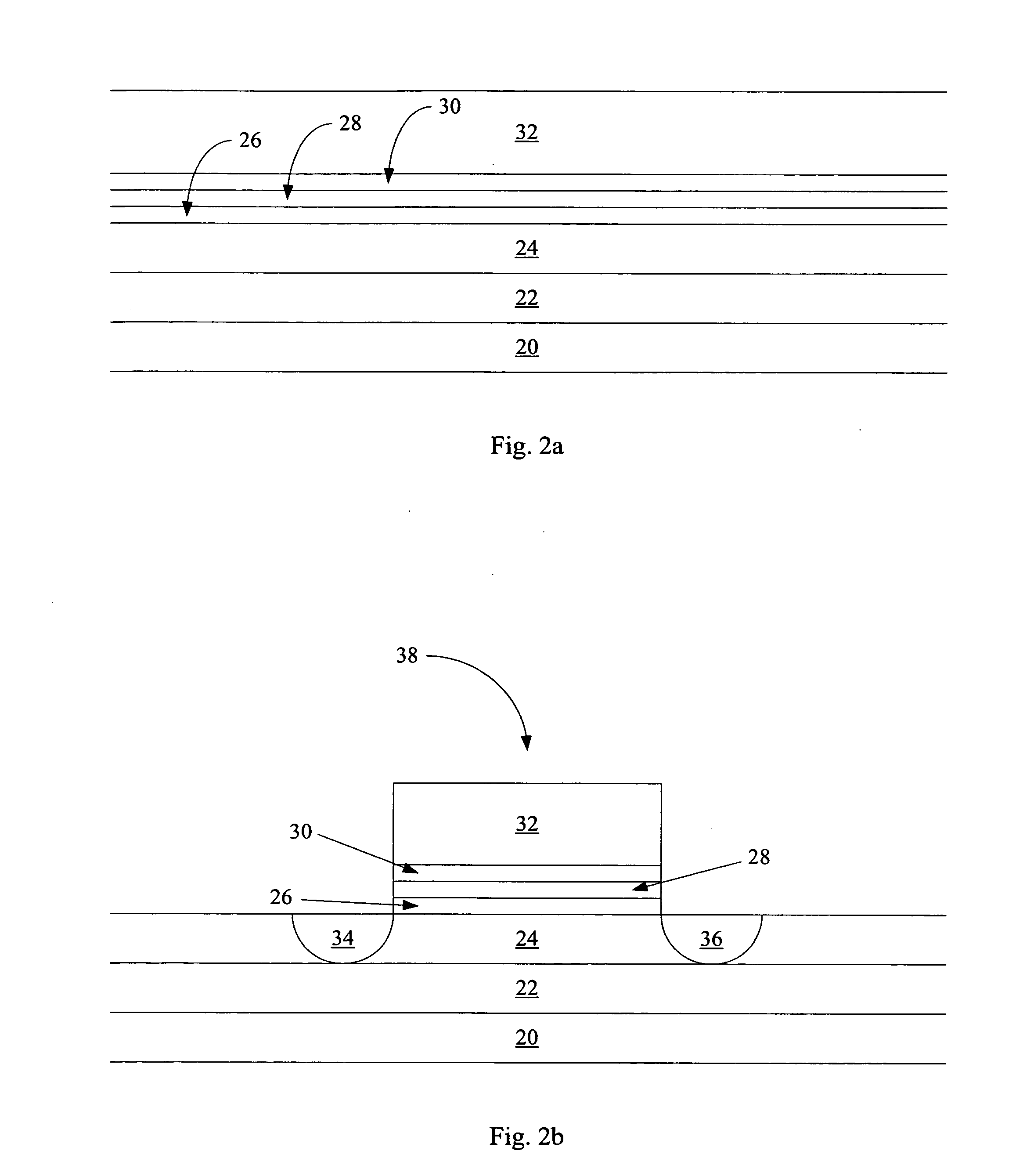
[0031] Formation of a thin film transistor according to the present invention begins with a substrate 20, shown in FIG. 2a. The substrate can be any suitable material. In some embodiments, it can be a monocrystalline silicon wafer. Circuitry, for example CMOS, can be formed in the wafer before fabrication of the thin film transistor begins. A dielectric layer 22, for example silicon dioxide, isolates subsequent layers from substrate 20. Layers 20 and 22 are a representation of one possibility; additional layers may be present, of course.

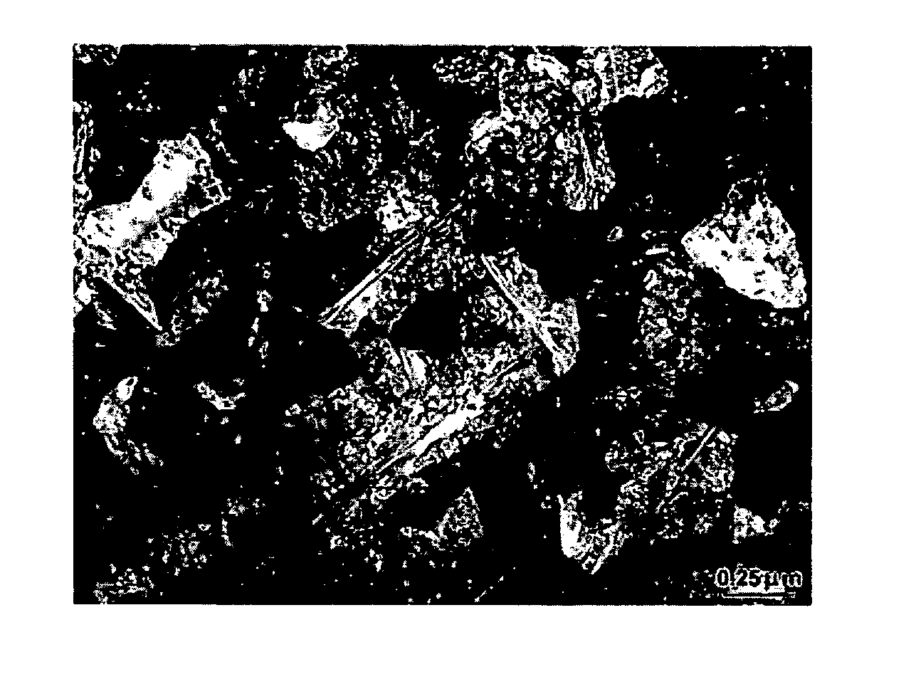
[0032] Silicon layer 24 is deposited by an LPCVD process. The layer should be in situ doped with a p-type dopant, preferably boron, and can be formed by simultaneously flowing a gas that will donate silicon atoms, for example silane (SiH4), and a gas that will donate boron atoms, for example BCl3, though other gases can be used. The silane can be flowed at any suitable rate, for example at 500 sccm, while the BCl3 should be provided at a very low ra...


PUM


Abstract

A method is disclosed to form a large-grain, lightly p-doped polysilicon film suitable for use as a channel region in thin film transistors. The film is preferably deposited lightly in situ doped with boron atoms by an LPCVD method at temperatures sufficiently low that the film is amorphous as deposited. After deposition, such a film contains an advantageous balance of boron, which promotes crystallization, and hydrogen, which retards crystallization. The film is then preferably crystallized by a low-temperature anneal at, for example, about 560 degrees for about twelve hours. Alternatively, crystallization may occur during an oxidation step performed, for example at about 825 degrees for about sixty seconds. The oxidation step forms a gate oxide for a thin film transistor device, for example a tunneling oxide for a SONOS memory thin film transistor device.

Description

BACKGROUND OF THE INVENTION [0001] The invention relates to a method for forming a large-grain polycrystalline silicon film for use in thin film transistors, the film doped with a p-type dopant. [0002] Thin film transistors are conventionally formed in silicon deposited over a substrate, often glass. Since the silicon is not epitaxially grown, it is not monocrystalline. Instead it is typically polycrystalline silicon, herein referred to as polysilicon. [0003] Transistors formed in single-crystal silicon have no grain boundaries in the channel region. However, when the channel region of a transistor is formed in a polysilicon layer, grain boundaries in the polysilicon tend to decrease carrier mobility, degrading device performance. It is advantageous, therefore, to increase grain size, decreasing the number of grain boundaries. [0004] Methods typically used to increase grain size include the introduction of catalysts, such as nickel or germanium, and laser annealing. Both of these me...

Claims


Application Information

Patent Timeline
IPC IPC(8): H01L21/00
CPCH01L21/2022H01L21/84H01L29/16H01L29/792H01L29/66833H01L29/78675H01L29/66757H01L21/0262H01L21/02592H01L21/02488H01L21/02532H01L21/02579H01L21/02672H01L21/02595H01L21/02381
Inventor GU, SHUONALLAMOTHU, SUCHETA
Owner SANDISK TECH LLC
Why Eureka
Try Eureka