Self-aligned contact etch with high sensitivity to nitride shoulder

a contact etching and high sensitivity technology, applied in the field of plasma etching of dielectric materials, can solve the problems of reducing the etching efficiency affecting the etching accuracy of the gate structure, so as to achieve the effect of reliably controlling the etching

Inactive Publication Date: 2006-03-09
APPLIED MATERIALS INC
View PDF11 Cites 243 Cited by
  • Summary
  • Abstract
  • Description
  • Claims
  • Application Information

AI Technical Summary

Benefits of technology

[0022] In yet another aspect, the present invention relates to a substrate equipped with an SAC structure comprising first and second gate structures disposed on a silicon substrate. The gate structures have a gap between them of less than about 0.25 microns, typically less than about 0.18 microns, and most typically less than about 0.14 microns, and are covered by a layer of silicon nitride. A layer of undoped oxide is disposed over the layer of silicon nitride, and a layer of doped silicon oxide is disposed between the layer of undoped oxide and the layer of silicon nitride. Typically, the layer of doped oxide is thick enough to cover the SAC structure. The structure may be advantageously employed

Problems solved by technology

During this process, it is extremely important that the nitride layer over the gate structures is not significantly reduced in thickness, since doing so increases the likelihood of an electrical shortage in the completed device and can seriously degrade its performance.
Unfortunately, the nitride layer on the shoulder of the gate structure is highly prone to thinning or “faceting” during the etching process, both because of its geometry and because of the length of time it is exposed to the etching plasma during the etching process.
Unfortunately, the efficacy of methodologies of the type disclosed in Hung et al. are seen to decrease with decreasing features sizes.
Unfortunately, the chemistries used in the main etch of Hung et al.
(most notably C4F6/Ar) provide insufficient selectivity for the thinner nitride layers required by devices having feature sizes less than about 0.25 microns, with the result that an unacceptable amount of faceting is found to occur in the corner nitride.
Moreover, while it might be theoretically possible to time the main etch of the field oxide layer so that it terminates before the corn

Method used


Image

  • Self-aligned contact etch with high sensitivity to nitride shoulder
  • Self-aligned contact etch with high sensitivity to nitride shoulder
  • Self-aligned contact etch with high sensitivity to nitride shoulder

Examples


example 1

[0065] This experiment demonstrates the etch stop behavior of Freon 134 on undoped oxide.

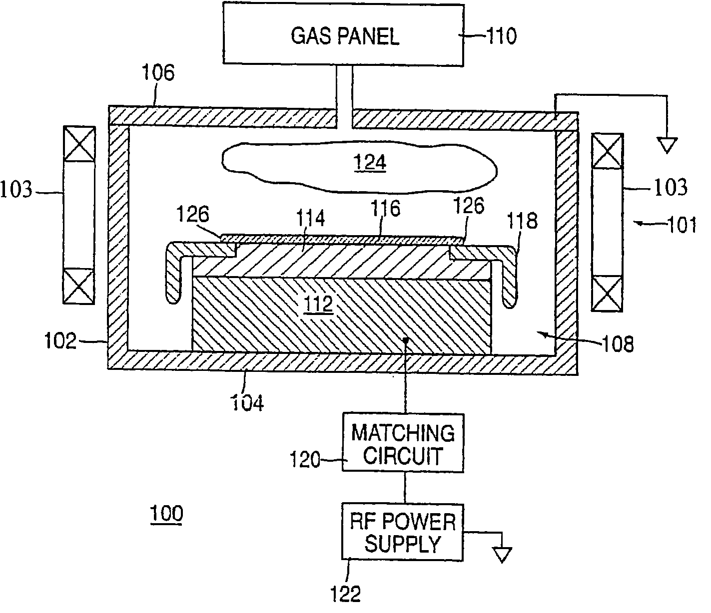
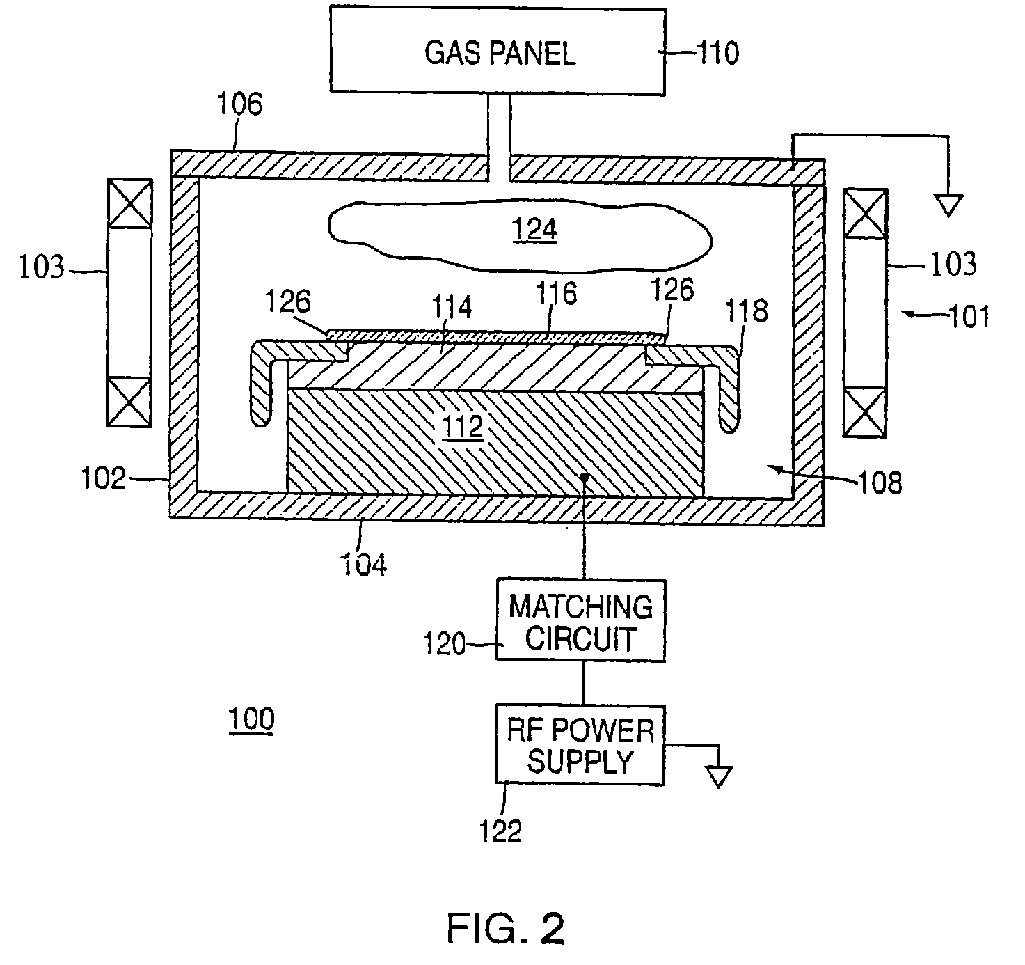
[0066] A wafer was provided which consisted of a surface layer of 9% PSG at the center of the wafer disposed on an undoped oxide substrate. Three separate holes were etched into the wafer using a MERIE reactor equipped with an eMAX chamber and using a gas stream consisting of C4F6Freon 134 / O2 / Ar. The processing parameters were as follows:

Chamber Pressure:40 to 80 mTorrPower used to generate plasma:1000 to 1800 wattsCathode Temperature:15 to 35° C.B-Field:0 to 50 GaussO2 flow rate:15 sccmFreon 134:2-8 sccmArgon flow rate:500 sccmC4F6 flow rate:20-30 sccm

[0067] The duration of the etch was approximately 60 to 90 seconds. The plasma readily penetrated the doped oxide surface layer, but exhibited etch stop behavior with respect to the underlying substrate.

example 2

[0068] This example illustrates the lack of selectivity Freon 134 exhibits with respect to flat nitride.

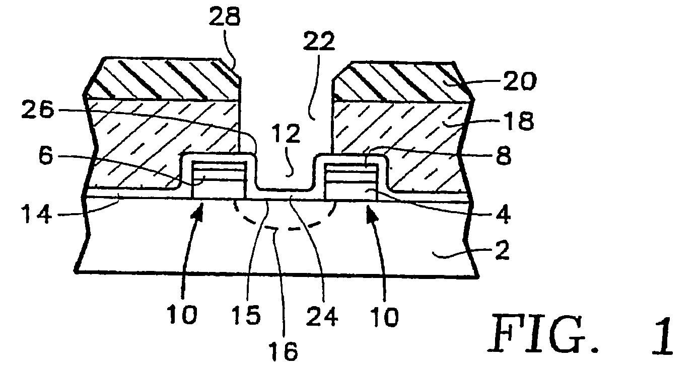
[0069] A wafer was provided which consisted of the following layer sequence:

MaterialThicknessDUV PRBARC700 ÅTEOS4000 Å BPSG4000 Å SiON Liner180 ÅPolygate

[0070] Using the methodology and apparatus of EXAMPLE 1, the undoped oxide layer 8 was etched using C4F6 / O2 / Ar chemistry at respective flow rate ratios of 25:15:500 until the BPSG layer was exposed.

[0071] Next, the chemistry was switched to Freon 134 / CHF3 / Ar at respective flow rate ratios of 6:80:90, and etching was continued. The plasma penetrated the flat nitride layer at the bottom of the gap, thus demonstrating lack of selectivity of Freon 134 to flat nitride.

example 3

[0072] This example illustrates the poor corner nitride selectivity exhibited by C4F6 / O2 / Ar only chemistry.

[0073] The experiment of EXAMPLE 2 was repeated, using different chemistry. C4F6 / O2 / Ar was used to etch through the TEOS layer with flow rates of 30 / 20 / 500, respectively. The etch was terminated after the plasma had penetrated the BPSG layer and had come into contact with the corner nitride. Next, C4F6 / O2 / Ar / Freon 134A was used to etch through the BPSG layer using flow rates of 27 / 15 / 500 / 9, respectively. The plasma exhibited etch stop behavior with respect to the flat nitride portion, thus demonstrating the selectivity of C4F6 / O2 / Ar / Freon 134A chemistry to flat nitride. However, the corner nitride was noticeably eroded where it had come into contact with the plasma during the first etching step, thus demonstrating that C4F6 / O2 / Ar only chemistry exhibits poor corner nitride selectivity.


PUM


Abstract

A method and apparatus are provided for etching semiconductor and dielectric substrates through the use of plasmas based on mixtures of a first gas having the formula CaFb, and a second gas having the formula CxHyFz, wherein a/b≧⅔, and wherein x/z≧½. The mixtures may be used in low or medium density plasmas sustained in a magnetically enhanced reactive ion chamber to provide a process that exhibits excellent corner layer selectivity, photo resist selectivity, under layer selectivity, and profile and bottom CD control. The percentages of the first and second gas may be varied during etching to provide a plasma that etches undoped oxide films or to provide an etch stop on such films.

Description

FIELD OF THE INVENTION [0001] This invention relates generally to plasma etching, and more particularly to plasma etching of dielectric materials using fluorochemicals. BACKGROUND OF THE INVENTION [0002] Oxides and nitrides are used widely in the manufacture of microprocessors and other semiconductor devices. Oxides are particularly useful, due to the ability to readily change the conductive properties of these materials from a dielectric state to a semiconducting state through ion implantation or through other commonly used doping methodologies. [0003] In many semiconductor manufacturing processes, the need arises to etch holes through one or more layers of doped or undoped oxide disposed in the proximity of a nitride layer. One example of this situation occurs during the manufacture of wafers equipped with Self-Aligned Contact (SAC) structures of the type depicted inFIG. 1. In such a construct, two gate structures 10 are formed on a silicon substrate 2 and are separated by a gap 1...

Claims


Application Information

Patent Timeline
IPC IPC(8): H01L21/302H01L21/461H01L21/311H01L21/60
CPCH01J37/3266H01L21/76897H01L21/31116H01L21/3065
Inventor JOSHI, AJEY M.NG, PUI MAN AGNESSTINNETT, JAMES A.DADU, USAMAREGIS, JASON M.
Owner APPLIED MATERIALS INC
Why Eureka
Try Eureka