Optically controlled electrical switching device based on wide bandgap semiconductors

a technology of wide bandgap semiconductors and switching devices, applied in electronic switching, pulse techniques, nanoinformatics, etc., can solve the problems of only being able to achieve substantial improvements, material quality and application markets have not been sufficiently mature until recently to justify significant manufacturing activities, and achieve greater power control efficiency. , the effect of high temperature operation

Inactive Publication Date: 2006-03-16
PETTIT JOHN W
View PDF13 Cites 43 Cited by
  • Summary
  • Abstract
  • Description
  • Claims
  • Application Information

AI Technical Summary

Benefits of technology

[0041] In the preferred embodiment, the NPN and PNP transistors can be made with conventional silicon technology, or more advantageously with large bandgap semiconductors including silicon carbide, SiC, or other wide bandgap semiconductors. The advantages of these wide bandgap semiconductors are numerous in power control applications and furthermore in military and aerospace applications, where greater power control efficiency and high temperature operation is extremely desirable.
[0042] This leads to another large advantage of this invention, namely the operation of this invention in an opticall

Problems solved by technology

Power switching devices are reaching fundamental limits imposed by the low breakdown field of silicon, and substantial improvements can only be achieved by going to semiconductors with a higher breakdown field.
While the inherent properties of these materials give them dramatic performance advantages over conventional semiconductors (e.g., Si and GaAs), the materials' quality and application markets have not been sufficiently mature until recently to justify significant manufacturing activities.
However, because of technological differences, power devices in SiC will be very different from silicon devices, and a direct translation of silicon concepts to SiC is not always possible.
However, these III-V nitride compounds do not possess a native oxide similar to SiO2, so true MOS devices will not be feasible.
In addition, the nitrides suffer from the lack of a suitable lattice-matched substrate for crystal growth, and hence the material is in a more primitive state of development than SiC.
Currently available optically controlled power switches in addition to being based on silicon and n

Method used


Image

  • Optically controlled electrical switching device based on wide bandgap semiconductors
  • Optically controlled electrical switching device based on wide bandgap semiconductors
  • Optically controlled electrical switching device based on wide bandgap semiconductors

Examples


Embodiment Construction

[0055] A preferred embodiment will be set forth in detail with respect to the drawings, in which like reference numerals refer to like elements throughout.

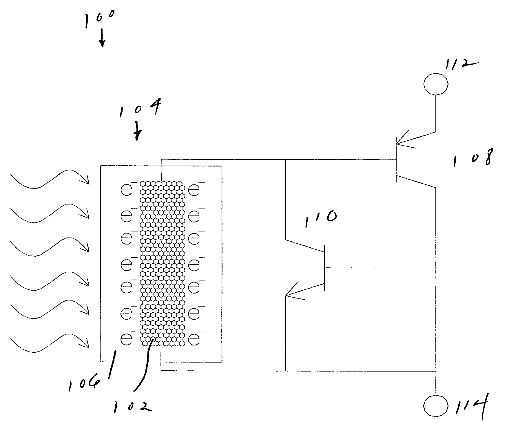
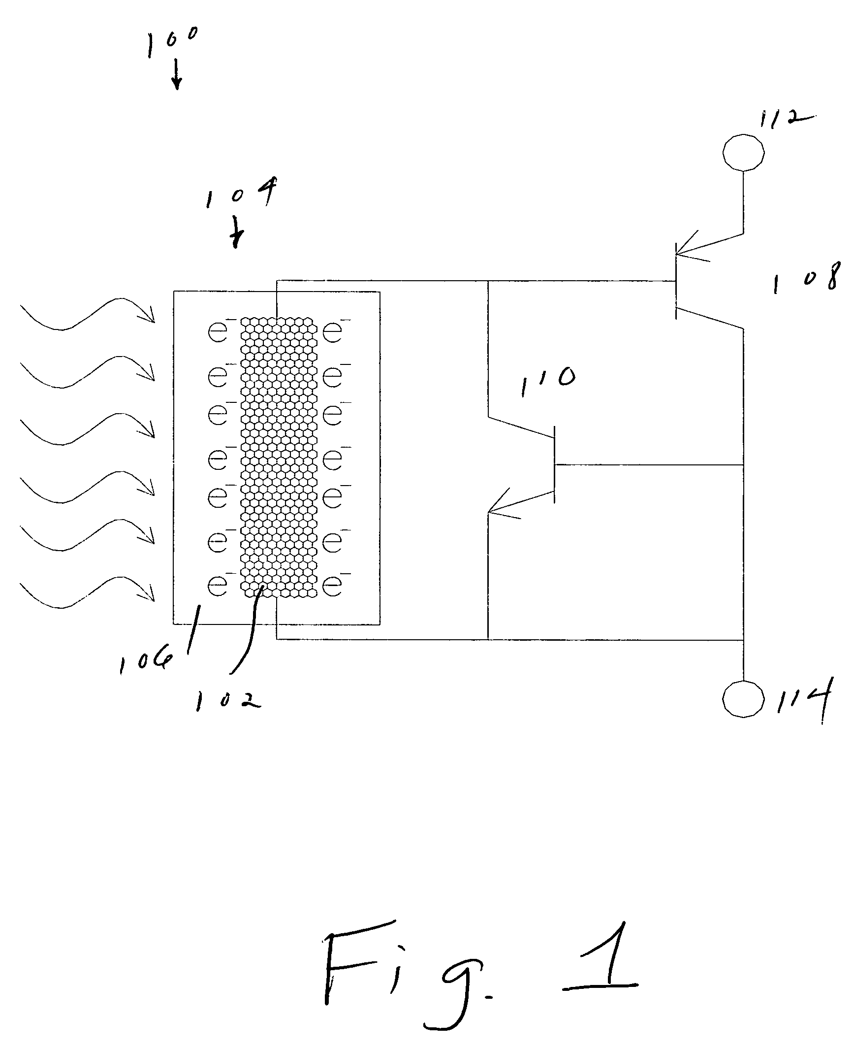
[0056]FIG. 1 shows a preferred embodiment of the switching device as 100. One or more semiconducting carbon nanotubes 102 form an optically gated FET 104 that in turn gates or switches on a power switching device. The power switching device has the topology of an SCR or IGBT, although other topologies can be implemented. The carbon nanotube FET 104 takes the place of the MOS FET in a customary IGBT arrangement. The carbon nanotube FET 104 is optically activated by light that is supplied by an optical fiber or any such optical means that creates charge near the nanotube surface when the light interacts with the photo-generating material 106 surrounding the carbon nanotube 102. This charge acting on the carbon nanotube surface is denoted by the e− symbols.

[0057] When the carbon nanotube 102 is made to conduct by the application of...


PUM


Abstract

A power switching device includes an optically controlled component using a semiconducting carbon nanotube. An optical signal transmitted over an optical fiber controls the conductivity of the nanotube. The nanotube transmits a signal controlled by the optical signal to a wide-bandgap semiconductor power switch, which switches the power.

Description

REFERENCE TO RELATED APPLICATION [0001] The present application claims the benefit of U.S. Provisional Patent Application No. 60 / 533,151, filed Dec. 31, 2003, whose disclosure is hereby incorporated by reference into the present disclosure.FIELD OF THE INVENTION [0002] The present invention is directed to an optically controlled switching device and more particularly to such a device which exploits the advantages of wide bandgap (WBG) semiconductors. DESCRIPTION OF RELATED ART [0003] Power switching devices are reaching fundamental limits imposed by the low breakdown field of silicon, and substantial improvements can only be achieved by going to semiconductors with a higher breakdown field. Wide bandgap semiconductors, such as silicon carbide, SiC, have a bandgap of around 3 eV and 8 times the breakdown voltage and 100-200 times the on state conductivity of silicon. SiC can work at temperatures of 600 degrees Centigrade, has much better thermal conductivity than silicon, has a coeff...

Claims


Application Information

Patent Timeline
IPC IPC(8): H01L31/111H01L31/10H01L31/11H01L51/00H01L51/42H03K17/78H03K17/795
CPCB82Y10/00B82Y20/00H01L2924/0002B82Y30/00H01L31/10H01L31/11H01L51/0048H01L51/0504H01L51/422H01L51/4253H01L51/428H03K17/78H03K17/795H01L2924/00H10K85/221H10K10/00H10K30/15H10K30/65H10K30/30
Inventor PETTIT, JOHN W.
Owner PETTIT JOHN W
Why Eureka
Try Eureka