

Method for manufacturing selective area grown stacked-layer electro-absorption modulated laser structure
- Summary
- Abstract
- Description
- Claims
- Application Information
AI Technical Summary
Benefits of technology
Problems solved by technology
Method used
Image

Examples
Embodiment Construction
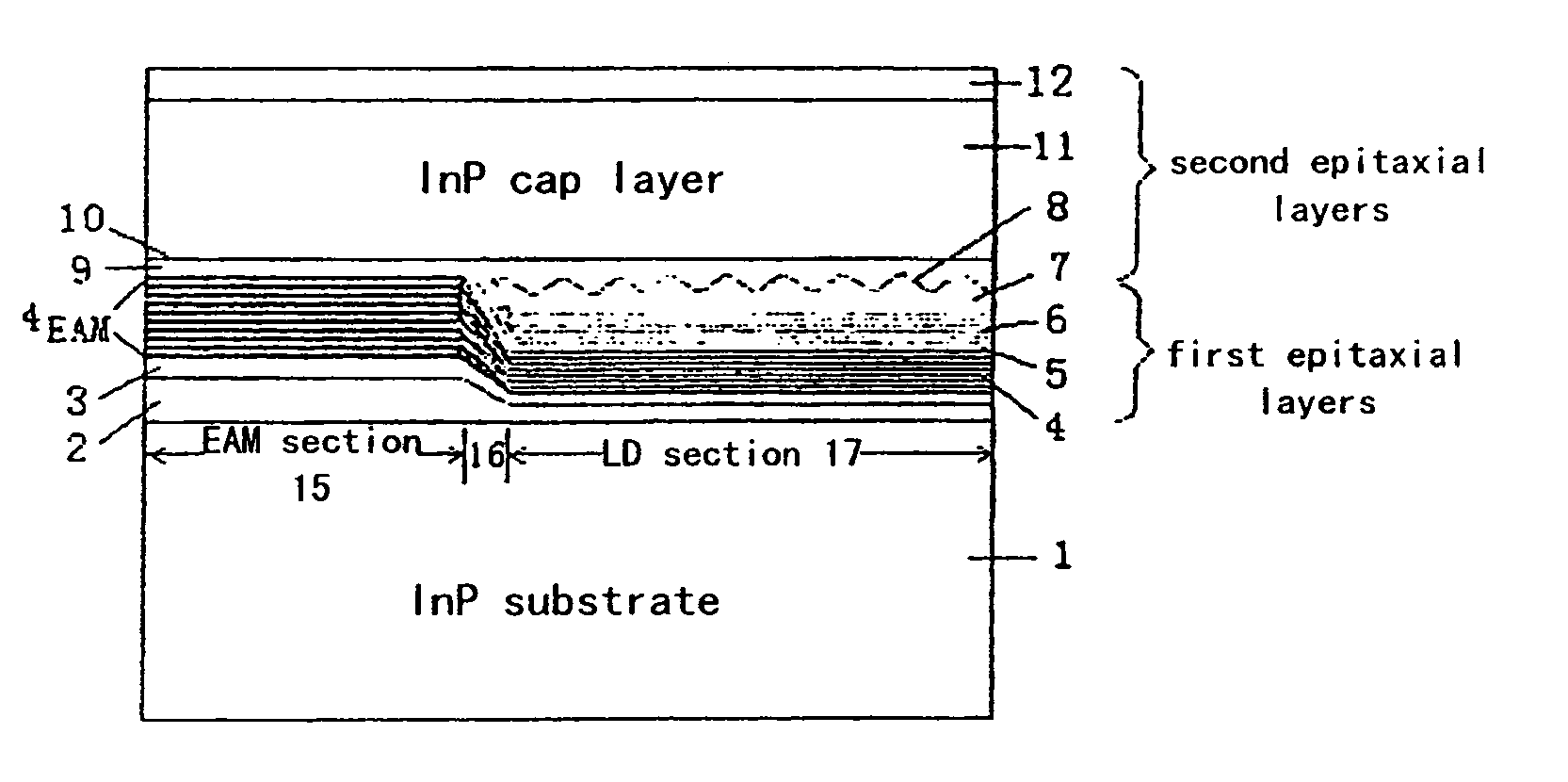
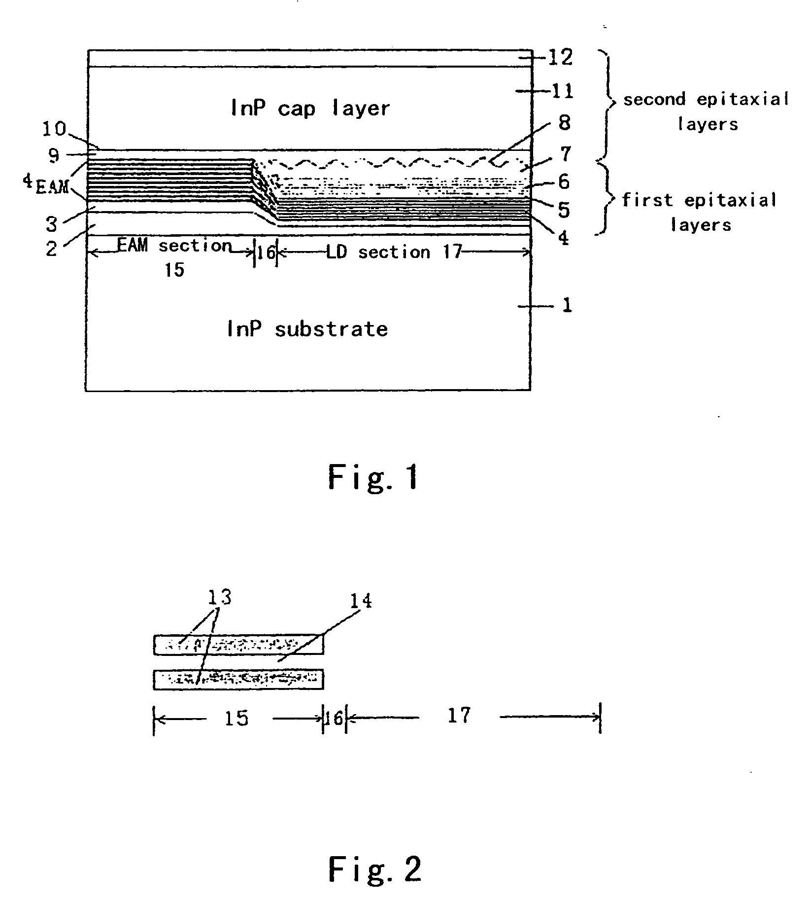
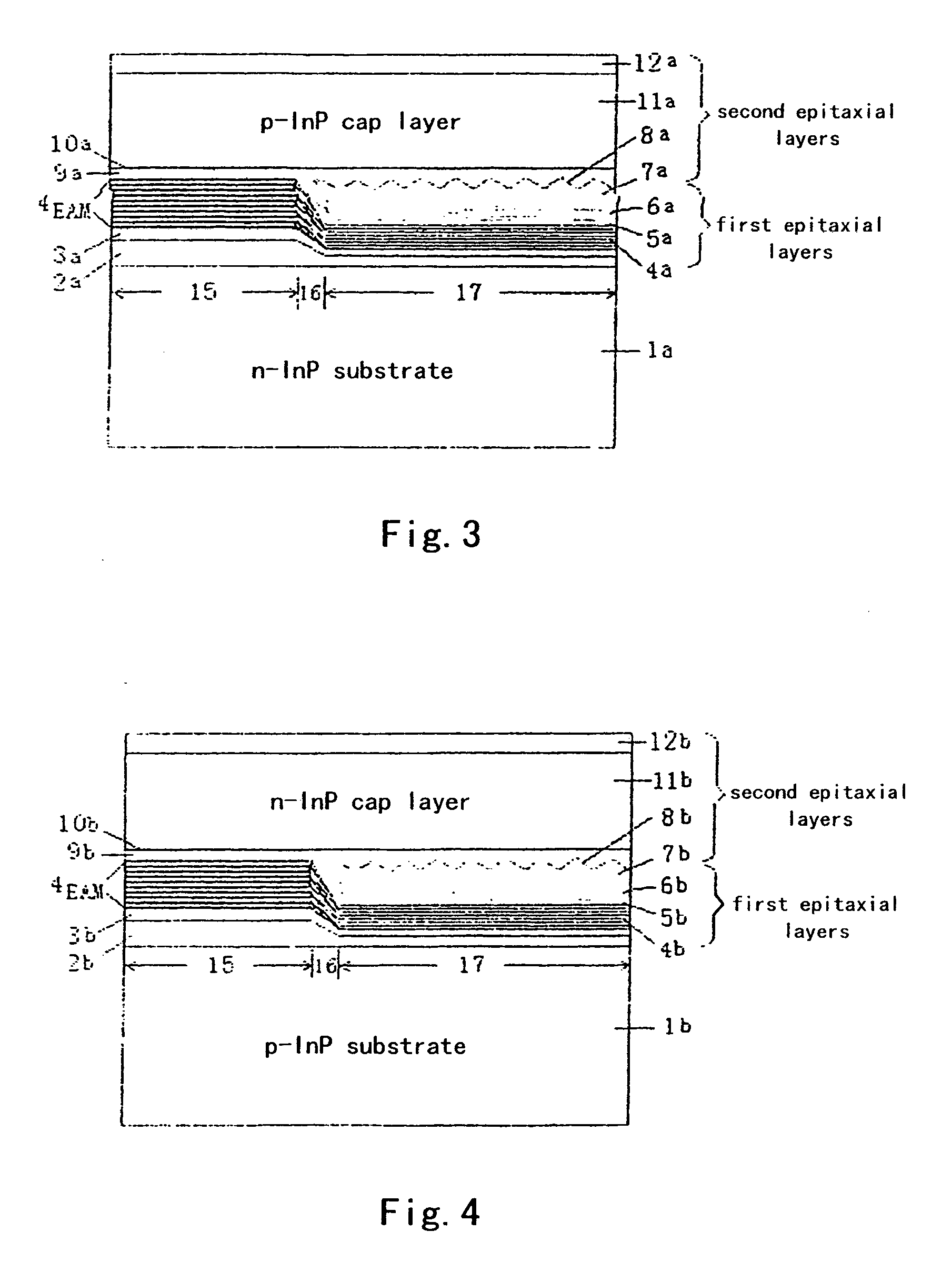
[0034] Referring to FIG. 1 and FIG. 2, a method for manufacturing a selective area grown stacked-layer electro-absorption modulated laser structure comprises following steps.
[0035] Step 1: a selective growth pattern of a modulator section 15 is formed on a substrate 1, wherein the selective growth pattern of the modulator 15 is two dielectric film stripes 13, which have a length of 100-300 μm and a width of 10-50 μm, an opening width 14 of the selective growth between the two dielectric stripes is 10-40 μm; wherein said dielectric film is of SiO2 or Si3N4, and has a thickness of 100-300 nm; wherein a length of the modulator section 15 is 100-300 μm, a length of a laser section 17 is 200-600 μm, and a transition region 16 between the modulator section 15 and the laser section 17 has a length of 30-100 μm, and the transition region 16 is also of a length of the electrically isolating section between the modulator and the laser;
[0036] Step 2: a 2-stacked-layer active region structure...
PUM
 Abstract
Description
Claims
Application Information