Capacitor device, electronic parts packaging structure, and method of manufacturing the capacitor device

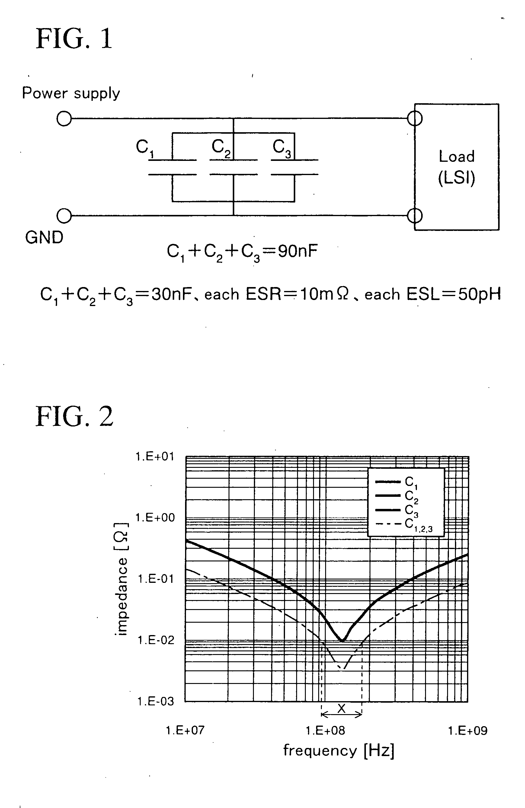
a capacitor and electronic parts technology, applied in capacitor manufacture, semiconductor/solid-state device details, capacitor manufacturing, etc., can solve the problems of unstable power-supply voltage of lsi, limit to the reduction of parasitic inductance, and inability to reduce the parasitic inductance, so as to reduce the thickness of the capacitor device, reduce packaging cost, and simplify the effect of electrical design

Active Publication Date: 2006-03-23
SHINKO ELECTRIC IND CO LTD
View PDF12 Cites 5 Cited by
  • Summary
  • Abstract
  • Description
  • Claims
  • Application Information

AI Technical Summary

Benefits of technology

[0011] It is an object of the present invention to provide a capacitor device capable of being applied to a decoupling capacitor that can reduce an impedance in a wide frequency band and can be suited to a higher frequency of electronic parts, an electronic parts packaging structure in which such capacitor device is built, and a method of manufacturing the capacitor device.

Problems solved by technology

In such digital LSIs, a power-supply voltage of the LSI is apt to become unstable when the impedance of the LSI is suddenly varied, and so forth.
However, there is a limit to the reduction in the parasitic inductance even though the wiring distance between the LSI chip and the capacitor is set to the shortest length.
Then, when the higher frequency of the LSI is further forwarded, such a situation is supposed that either the power-supply voltage of the LSI becomes unstable or the malfunction of the LSI is caused by the high-frequency noise.

Method used


Image

  • Capacitor device, electronic parts packaging structure, and method of manufacturing the capacitor device
  • Capacitor device, electronic parts packaging structure, and method of manufacturing the capacitor device
  • Capacitor device, electronic parts packaging structure, and method of manufacturing the capacitor device

Examples


first embodiment

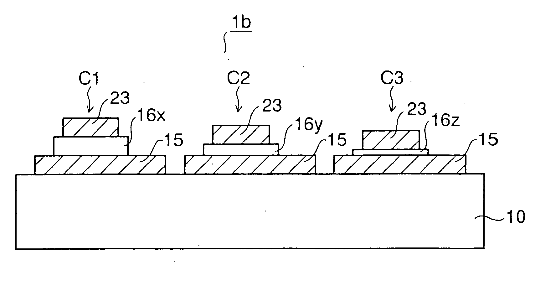
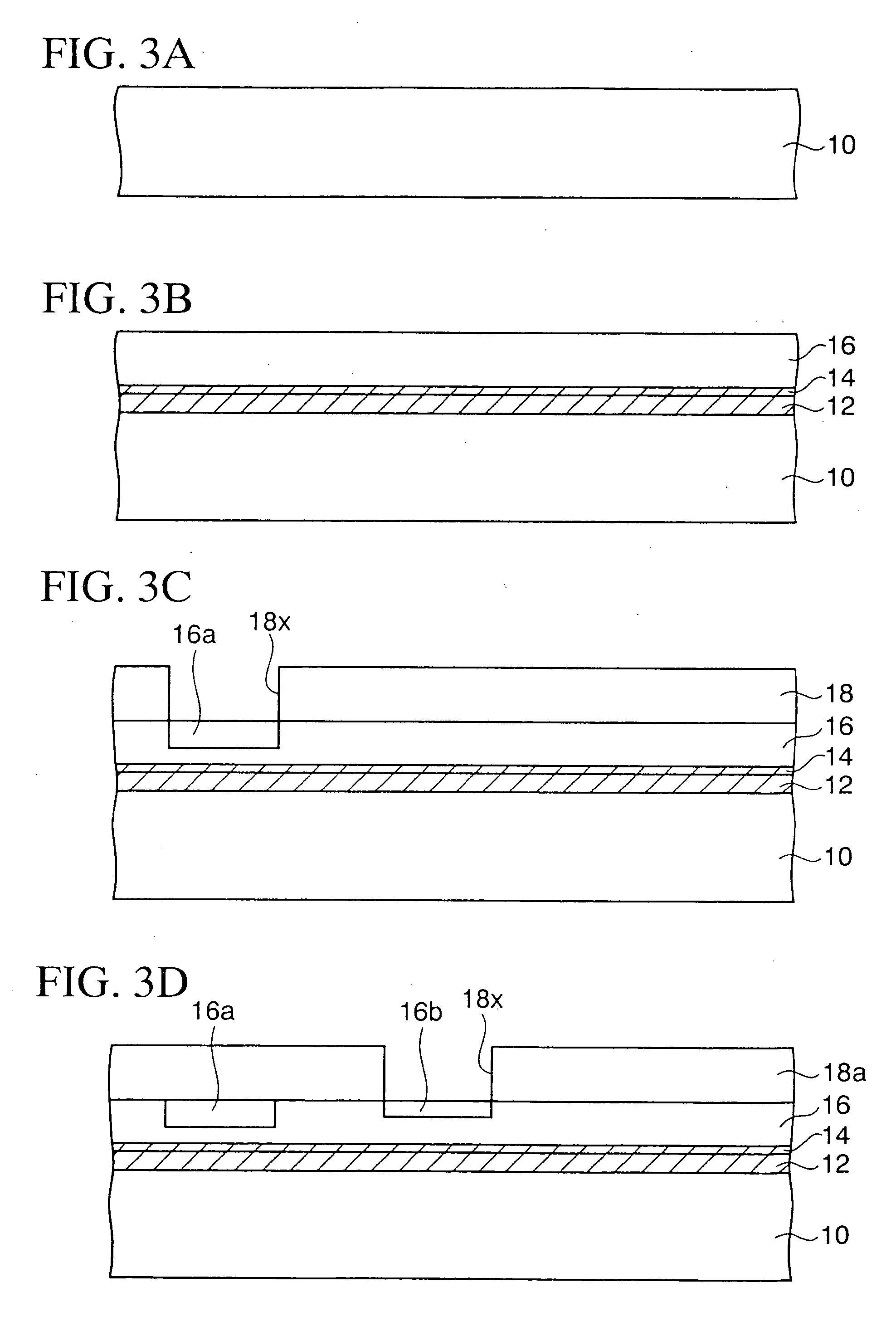
[0038] Next, a capacitor device according to a first embodiment of the present invention will be explained hereunder. FIGS. 3A to 3J are sectional views showing a method of manufacturing a capacitor device according to a first embodiment of the present invention in sequence.

[0039] First, as shown in FIG. 3A, a core substrate 10 made of silicon, glass, ceramic, resin, or the like, or a metal such as iron-nickel alloy, aluminum, or the like is prepared. In the case where a resin substrate is used as the core substrate 10, it is preferable that the resin containing fillers such as silica and having a coefficient of thermal expansion of 5 to 30 ppm / K should be employed.

[0040] Also, when the thin-type capacitor device is manufactured, the core substrate 10 having a thickness of 50 μm or less is employed. When the thin-type core substrate 10 is employed, the core substrate may be fixed to the supporting member and then the supporting member may be removed after manufacturing steps are e...

second embodiment

[0100]FIGS. 9A to 9C are sectional views showing a method of manufacturing a capacitor device according to a second embodiment of the present invention. A difference of the second embodiment from the first embodiment is that a method of forming the dielectric film is different. Detailed explanation of the same steps as those in the first embodiment will be omitted herein.

[0101] First, as shown in FIG. 9A, the conductive film 12 is formed on the core substrate 10. Then, a first dielectric film pattern 16x is formed in the portion of the conductive film 12 in which the dielectric film of the first capacitor is formed. As a method of forming the first dielectric film pattern 16x, there is a lift-off method, for example. More particularly, first a resist film (not shown) having an opening portion in a predetermined portion is patterned. Then, a dielectric film such as a tantalum oxide film, or the like is formed on the resist film and in the opening portion by the sputtering method, or...


PUM

PropertyMeasurementUnit
frequencyaaaaaaaaaa
thicknessaaaaaaaaaa
thicknessaaaaaaaaaa

Abstract

In a capacitor device of the present invention includes a substrate, a plurality of lower electrodes formed on the substrate, a plurality of dielectric films formed on a plurality of lower electrodes respectively in a state that the dielectric films are separated mutually, and upper electrodes formed on a plurality of dielectric films respectively, a plurality of capacitors each composed of the lower electrode, the dielectric film, and the upper electrode are arranged on the substrate respectively, and each of the dielectric films in a plurality of capacitors has a different film thickness.

Description

RELATED APPLICATIONS [0001] This application is a divisional application of U.S. application Ser. No. 11 / 020,062, filed Dec. 23, 2004, which claims priority under 35 U.S.C. § 119 of Japanese Application No. 2003-430568, filed Dec. 25, 2003, all of which are incorporated herein by reference.BACKGROUND OF THE INVENTION [0002] 1. Field of the Invention [0003] The present invention relates to a capacitor device, an electronic parts packaging structure, and a method of manufacturing the capacitor device and, more particularly, a capacitor device capable of being applied to a decoupling capacitor that is arranged on a circuit substrate on which high-speed operated electronic parts are mounted to stabilize a power supply voltage and also reduce a high-frequency noise, an electronic parts packaging structure in which such capacitor device is built, and a method of manufacturing the capacitor device. [0004] 2. Description of the Related Art [0005] In recent years, reduction in the power-supp...

Claims


Application Information

Patent Timeline
Patent Type & Authority Applications(United States)
IPC IPC(8): H01G4/06H01G4/008H01G4/10H01G4/228H01G4/33H01G4/38H01G13/00H01G13/06H01L21/822H01L23/498H01L23/50H01L27/04H05K1/16H05K1/18
CPCH01L2924/01078Y10T29/43H01L2924/09701H01L2924/15311H01L2924/3011H05K1/162H05K2201/0191H05K2201/09509H05K2203/0315H05K2203/1476H01G4/10H01G4/38H01L23/49816H01L23/50H01L2224/16H01L2924/01019Y10T29/417Y10T29/435H01L2924/01079
Inventor YAMASAKI, TOMOO
Owner SHINKO ELECTRIC IND CO LTD
Why Eureka
Try Eureka