Method of forming improved rounded corners in STI features

a technology of sti and rounded corners, which is applied in the direction of semiconductor/solid-state device manufacturing, basic electric elements, electric apparatus, etc., can solve the problems of compromising device functionality, consuming a significant amount of power, and increasing the difficulty of electrical isolation of semiconductor devices, so as to achieve improved electrical isolation performance

Inactive Publication Date: 2006-03-23
TAIWAN SEMICON MFG CO LTD
View PDF7 Cites 22 Cited by
  • Summary
  • Abstract
  • Description
  • Claims
  • Application Information

AI Technical Summary

Benefits of technology

[0007] To achieve the foregoing and other objects, and in accordance with the purposes of the present invention, as embodied and broadly described herein, the present invention provides a method for forming a shallow trench isolation (STI) structure with improved electrical isolation performance.

Problems solved by technology

The art of electrically isolating semiconductor devices has become an increasingly difficult and important aspect in forming CMOS, DRAM, and SRAM devices including MOSFETS to ensure proper operation.
With the high integration of the semiconductor devices, improper electrical isolation among devices will cause current leakage, consuming a significant amount of power as well as compromising device functionality.
Among some examples of reduced functionality include latch-up, noise margin degradation, Voltage threshold shift, cross-talk, and excessive power usage.
As integrated circuit characteristic dimensions continue to be scaled down, it has become increasingly difficult to form STI trench rounded corners with the desired profiles necessary to prevent current leakage.
In addition, current leakage at or around STI features is increasingly sensitive to STI trench profiles as device sizes scale down.

Method used


Image

  • Method of forming improved rounded corners in STI features
  • Method of forming improved rounded corners in STI features
  • Method of forming improved rounded corners in STI features

Examples


Embodiment Construction

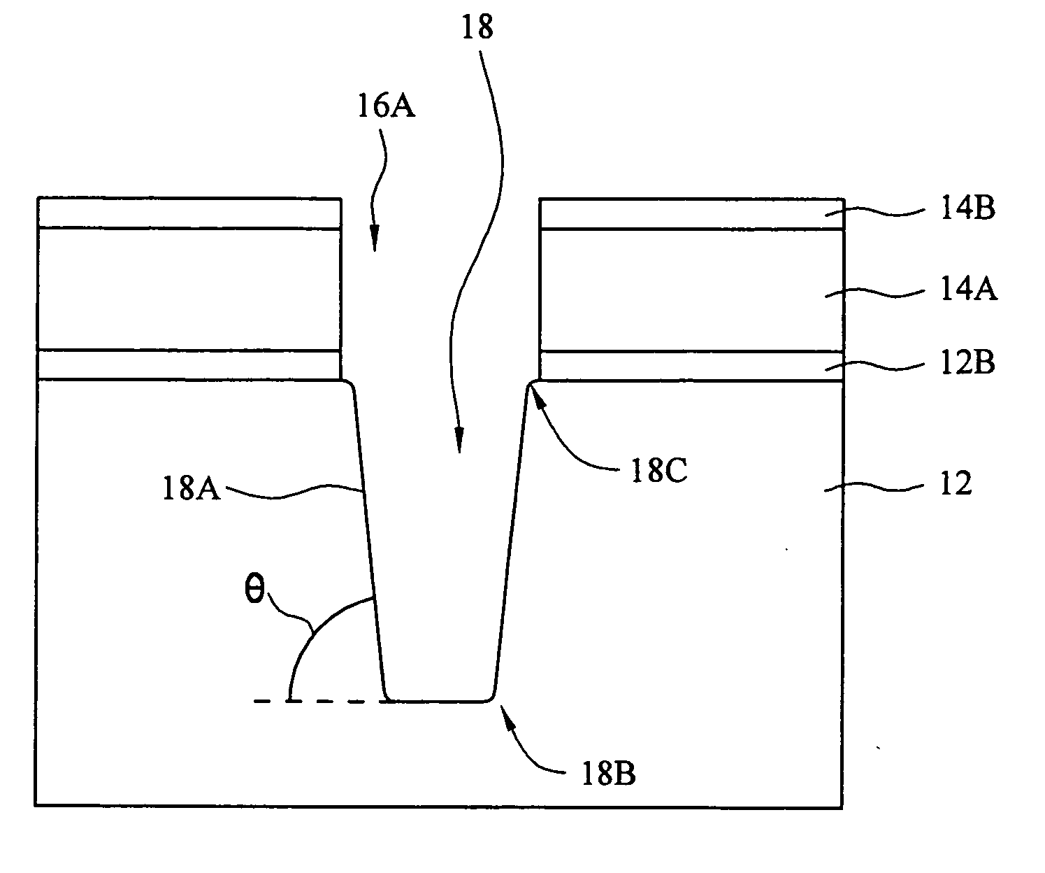
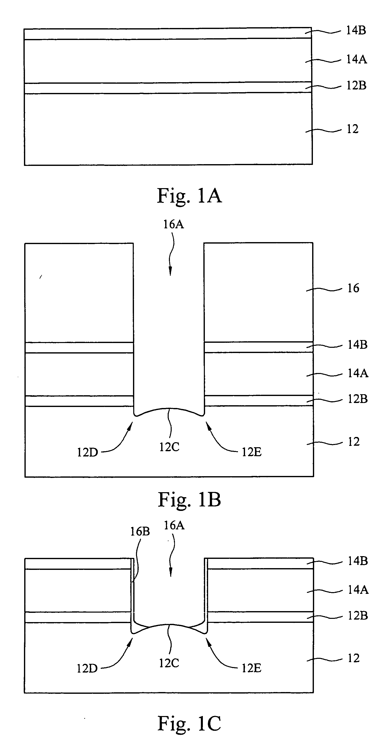
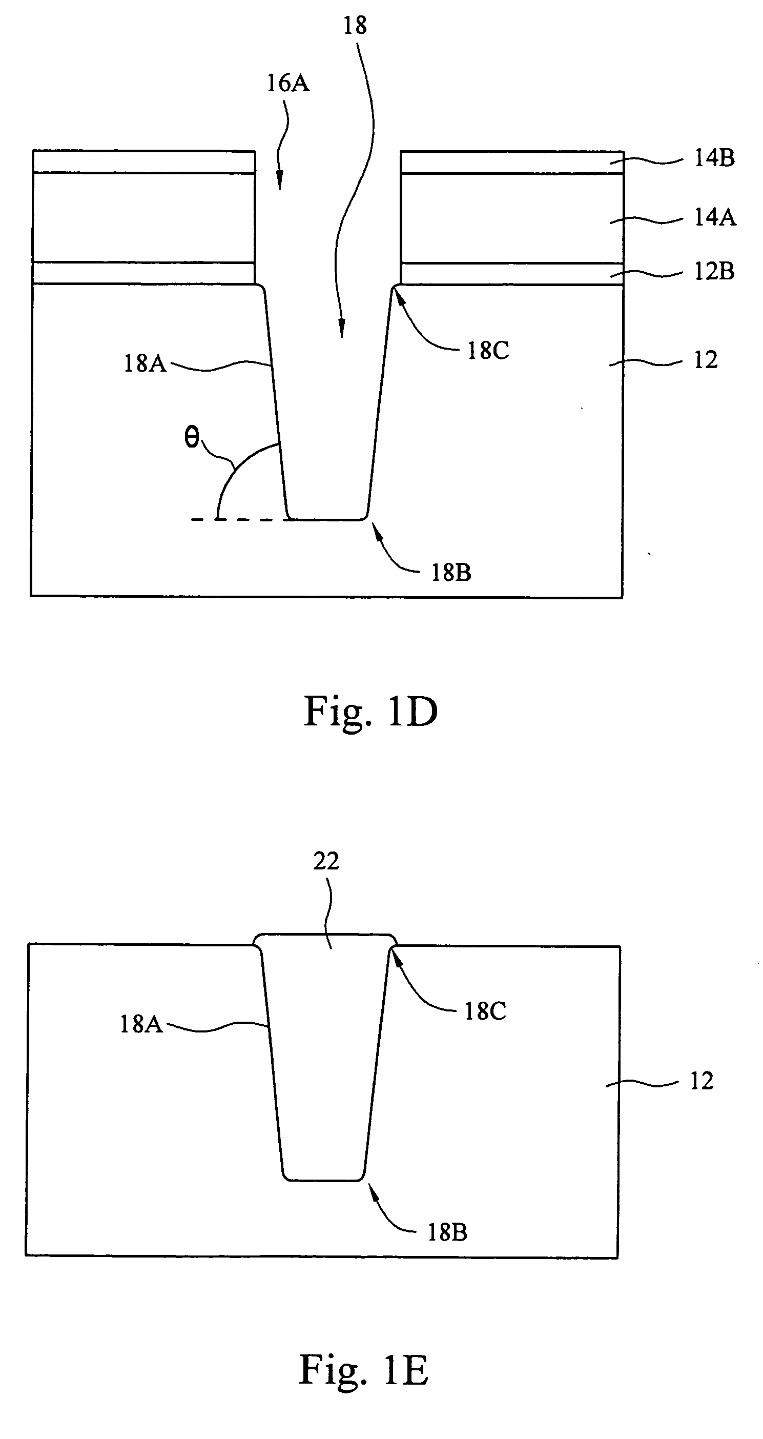
[0012] The method of the present invention is explained with respect to processing steps included in forming shallow trench isolation (STI) structures. It will be appreciated that the method of the present invention is particularly applicable to, but not limited to the formation of integrated circuits with characteristic dimensions less than about 0.25 microns, including less than about 0.13 microns. In addition, it will be appreciated that realized benefits of the present invention include avoiding electrical current (charge) leakage in a subsequently completed semiconductor device thereby improving subsequent device performance and reliability including device performance of CMOS, DRAM, SRAM and MOSFETS devices.

[0013] In one exemplary implementation of the present invention, referring to FIG. 1A is shown a semiconductor substrate 12, for example silicon. For example, the substrate 12 may include, but is not limited to silicon, strained semiconductor, compound semiconductor, multi...


PUM


Abstract

A method for forming a shallow trench isolation (STI) structure with improved electrical isolation performance including providing a semiconductor substrate including an overlying silicon oxide layer on the semiconductor substrate and a hardmask layer on the silicon oxide layer; dry etching in a first etching process to form a patterned hardmask opening for etching an STI opening; dry etching in a second etching process the semiconductor substrate to form an upper portion of an STI opening to form a polymer layer along sidewall portions of the STI opening; and, dry etching in a third etching process the STI opening to form rounded bottom corners and rounded top corners.

Description

FIELD OF THE INVENTION [0001] This invention generally relates to semiconductor processing methods and more particularly to a method for forming shallow trench isolation (STI) structures including improved rounded top and bottom corner profiles to avoid electrical charge leakage and improve electrical isolation in semiconductor devices. BACKGROUND OF THE INVENTION [0002] The art of electrically isolating semiconductor devices has become an increasingly difficult and important aspect in forming CMOS, DRAM, and SRAM devices including MOSFETS to ensure proper operation. Generally, every FET device must be electrically isolated from other devices to ensure that it operates without electrical interference from other devices. With the high integration of the semiconductor devices, improper electrical isolation among devices will cause current leakage, consuming a significant amount of power as well as compromising device functionality. Among some examples of reduced functionality include ...

Claims


Application Information

Patent Timeline
Patent Type & Authority Applications(United States)
IPC IPC(8): H01L21/76
CPCH01L21/76235H01L21/76232
Inventor CHEN, PO-JENLEU, JEN-HSIANGLIU, YAN-CHANG
Owner TAIWAN SEMICON MFG CO LTD
Why Eureka
Try Eureka