Self-reflowing printed circuit board and application methods

a printed circuit board and self-reflow technology, applied in the field of new printed circuit boards, can solve the problems of requiring rework, increasing the cost of the final product, generating rejections, etc., and achieves the effects of reducing the cost of the manufactured product, reducing the temperature exposure, and being easy to integra

Inactive Publication Date: 2006-03-30
TRUCCO HORACIO ANDRES
View PDF1 Cites 40 Cited by
  • Summary
  • Abstract
  • Description
  • Claims
  • Application Information

AI Technical Summary

Benefits of technology

[0012] The general objective of this invention is to provide the electronic manufacturing, or electronic packaging, industry with a new, safe, reliable, speedier, useful and, above all, a more economical process and means for soldering components to a PCB.
[0013] Because this invention only heats the component's leads or terminations to be joined by solder to a PCB while the rest of said component (namely its casing or housing) remains relatively cold, utilization of this invention will help to reduce manufactured-product cost because components rated to tolerate much lower temperature exposure (than now required by the oven reflow soldering proces

Problems solved by technology

This process exhibit inherit disadvantages that, indeed, increase the cost of the final product, generate rejects, require rework and reduce the reliability of the final product.
The electronic manufacturing industry accepts these inherit drawbacks and shortcomings, and works around them, for lack of a more suitable soldering process.
Therefore, all electronic components must be unnecessarily temperature-overrated to tolerate or survive the soldering process.
This requirement for high-temperature-exposure survival increases the cost of every component to be soldered to a PCB.
During the oven reflow soldering process, thermal shock (due to a fast heating rate) can crack certain components, in particular ceramic capacitors, increasing rejects and/or requiring costly rework.
Fast heating of plastic IC pa

Method used


Image

  • Self-reflowing printed circuit board and application methods
  • Self-reflowing printed circuit board and application methods
  • Self-reflowing printed circuit board and application methods

Examples


Embodiment Construction

[0076] Now, aided by FIGS. 1 through 8, components that form part of the fundamental embodiment of this invention shall be illustrated and described. Because the additional embodiments that permit practical utilization of the fundamental embodiment of the invention also include items-of-commerce recognized as public-domain prior art, those preferred embodiments will be illustrated afterwards in FIG. 9 and FIG. 11 and described in the next part of this specification.

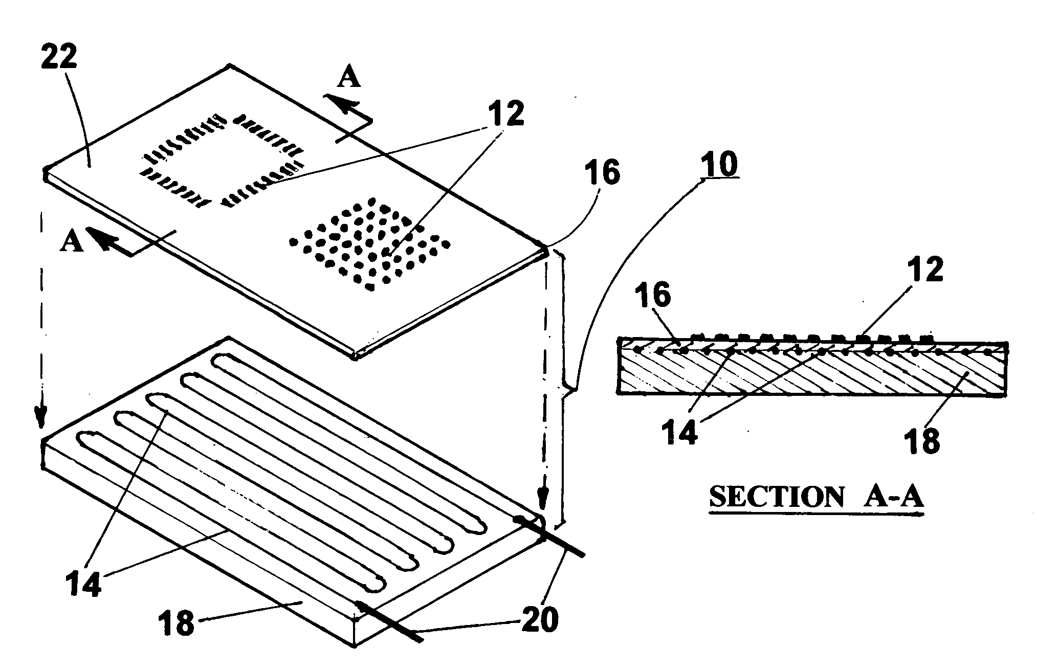
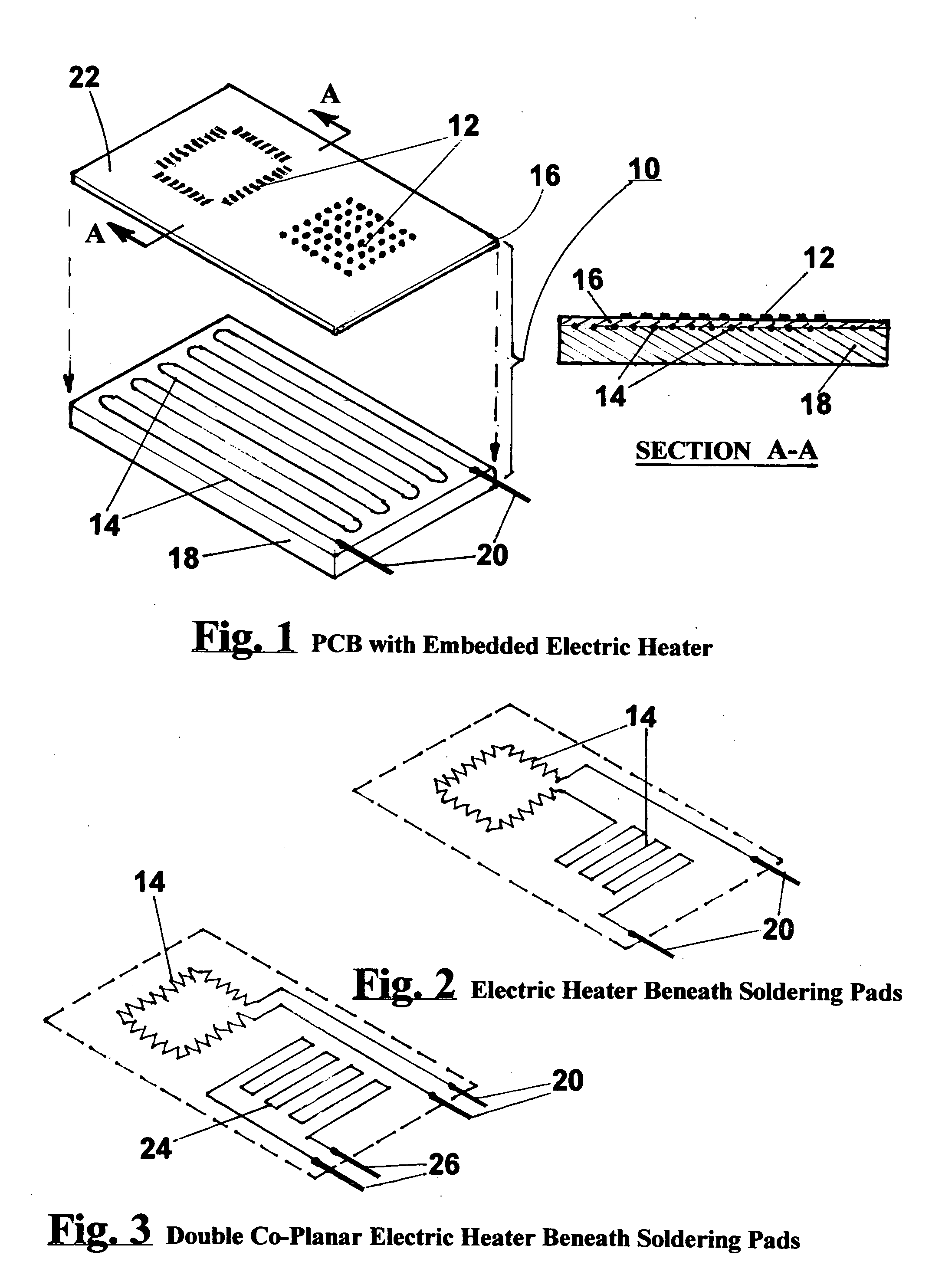
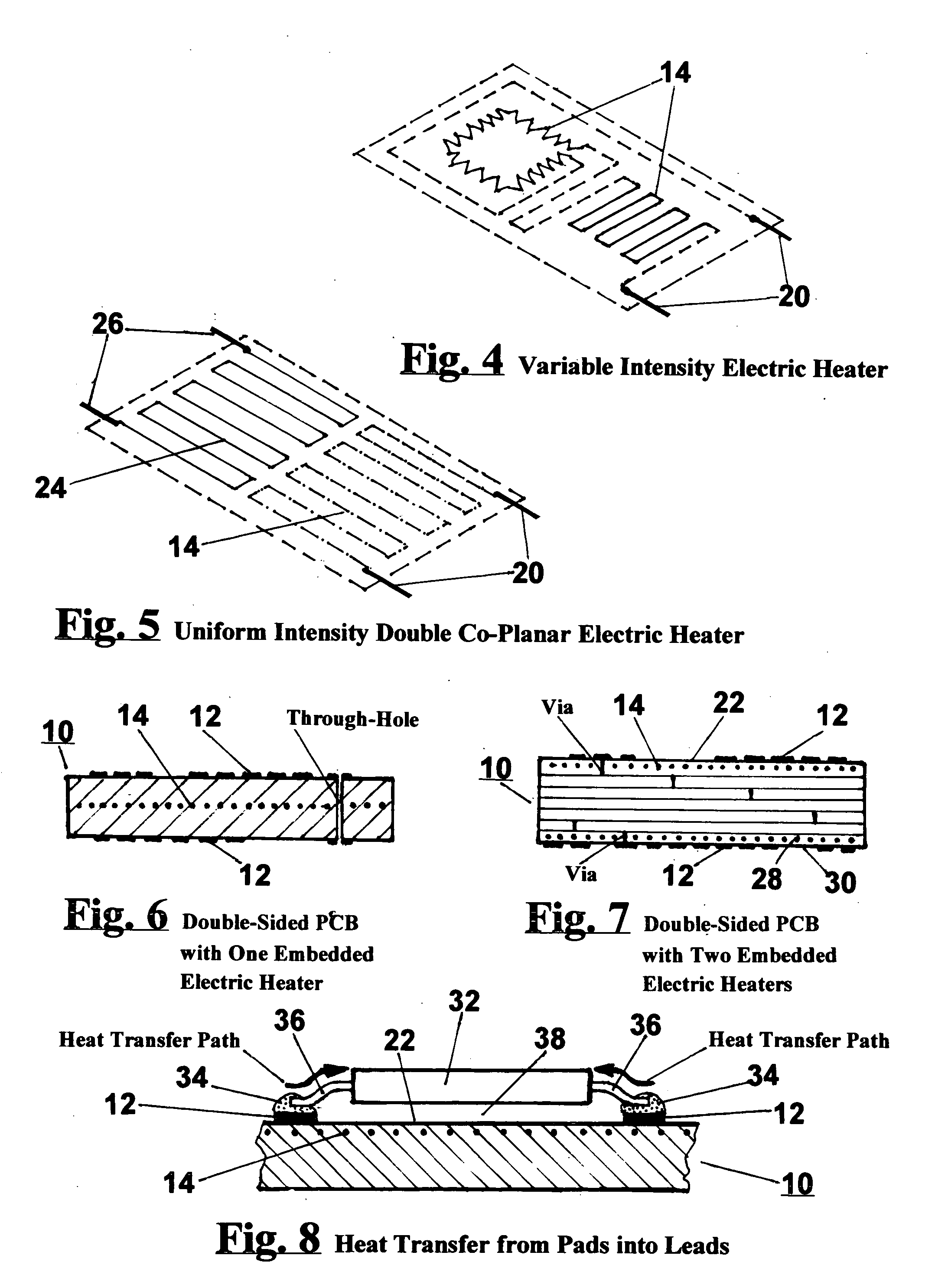
[0077]FIG. 1 shows in, both, exploded and sectional views the fundamental embodiment, namely a printed circuit board with embedded electric heater 10 (PCBwEEH 10) constructed according to this invention. To avoid clutter in the figure only two sets of soldering pads 12 are depicted, corresponding to the footprints of a QFP and a BGA packages. An electric heater 14 is embedded in a sandwich fashion between a top dielectric layer 16 and a bottom dielectric layer 18. Electric heater 14 has a pair of current supply leads 20-...


PUM


Abstract

A novel printed circuit board (PCB) 10 that incorporates embedded into its substrate an electric heater 14 is disclosed. This electric heater 14 becomes the only source of heat for simultaneously soldering components to pads 12. The PCB 10 is the key element that permits to create apparatuses and implement processes for soldering PCB assemblies without utilizing a reflow oven. Compared against the prior art this invention requires less manufacturing equipment, reduces the manufacturing cost, reduces manufacturing energy consumption and improves the quality and reliability of soldered PCB assemblies.

Description

FIELD OF INVENTION [0001] This invention relates to a novel printed circuit board (PCB) that incorporates an embedded electric heater into its substrate. Said electric heater becomes the only source of heat that allows to attain a self-reflowing process for simultaneously soldering multiple electronic components to said PCB face. BACKGROUND-DESCRIPTION OF THE PRIOR ART [0002] The manufacture of most modern electronic products require a PCB that allows to electrically interconnect a variety of electronic components and also holds them together in a relatively rigid condition. Many types of components are placed over a PCB such as; resistors, capacitors, inductors, transformers, integrated circuit (IC) packages, connectors, headers, RF shields, LEDs, switches, board interface systems, battery sockets, etc. that are electrically connected and restrained by means of soldered joints either over one side or both sides of a PCB. These joints can be attained by three methods: hand soldering...

Claims


Application Information

Patent Timeline
IPC IPC(8): H05K7/20H05B3/16
CPCH01L2224/81234H01L2924/12041H01L2924/19107H05K1/0212H05K3/3494H05K2201/10287B23K3/0307B23K2201/42H01L24/97H01L24/98H01L2224/16225H01L2924/01005H01L2924/01006H01L2924/01019H01L2924/01033H01L2924/01075H01L2924/01082H01L2924/14H01L2224/05573H01L2224/05568H01L2924/00014H01L2224/0554B23K2101/42H01L2924/00H01L2224/05599H01L2224/0555H01L2224/0556
Inventor TRUCCO, HORACIO ANDRES
Owner TRUCCO HORACIO ANDRES
Why Eureka
Try Eureka