

Nitride based semiconductor device and method for manufacturing the same
a technology of nitride and semiconductor, which is applied in the direction of semiconductor devices, electrical devices, impedence networks, etc., can solve the problems of deteriorating surface characteristics, degrading crystallinity in the vicinity of heterostructure, and deteriorating surface characteristics of saw filters, so as to improve crystallinity, improve electrical properties, and improve the effect of surface characteristics
- Summary
- Abstract
- Description
- Claims
- Application Information
AI Technical Summary
Benefits of technology
Problems solved by technology
Method used
Image

Examples
Embodiment Construction
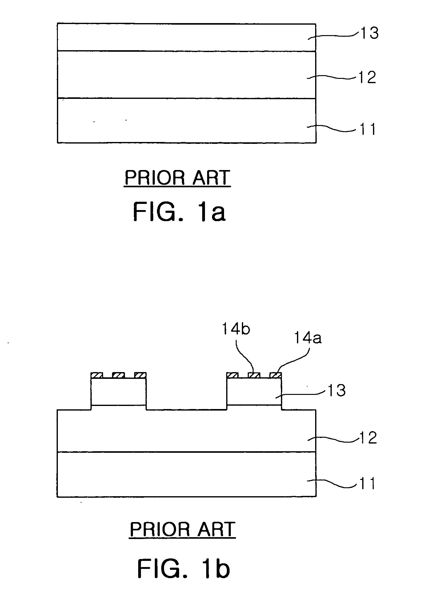
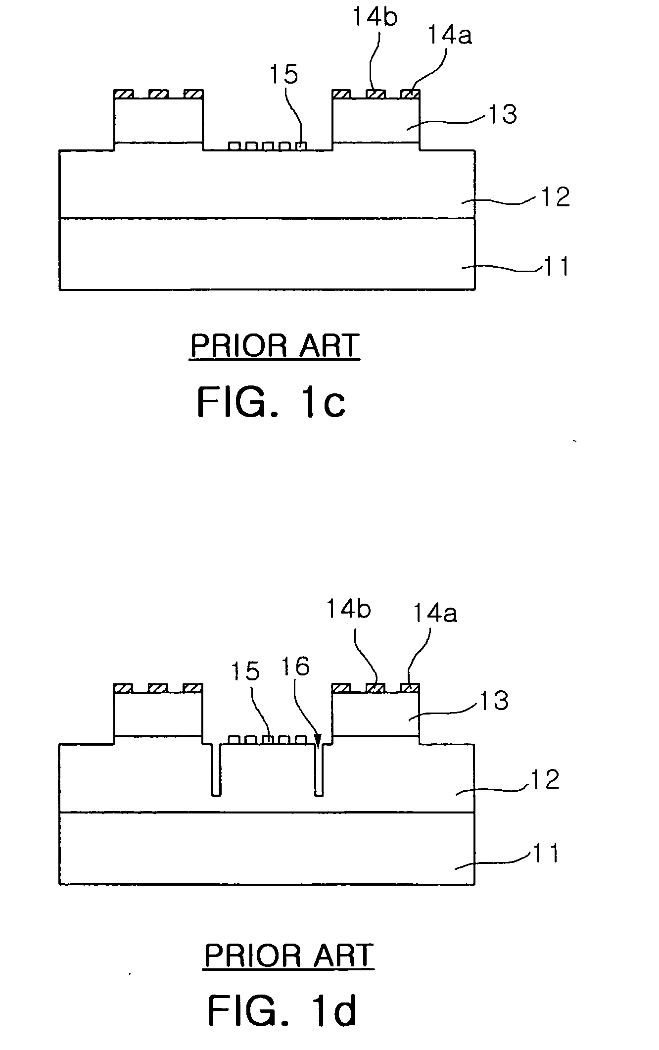
[0028] Detailed description will be made of embodiments of the present invention with reference to the accompanying drawings. However, various modifications to the embodiments of the present invention may easily be made, and the scope of the present invention is not limited by the following embodiments. These embodiments are provided to those skilled in the art for a better understanding of the present invention. In the drawings, the shape and size of elements may be exaggerated for the purpose of clarity, and the same elements are denoted by the same reference numerals even though they are depicted in different drawings.
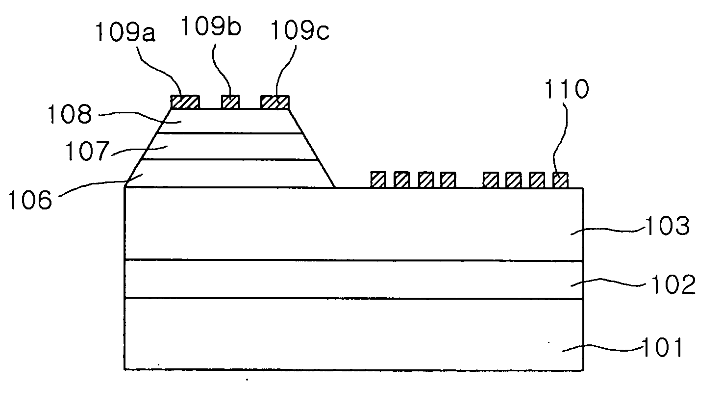
[0029]FIG. 2 is a cross-sectional view showing the structure of a nitride-based semiconductor device according to one embodiment of the present invention, and FIG. 3 is a top view of the nitride-based semiconductor device shown in FIG. 2. Specifically, FIG. 2 is a cross-sectional view of FIG. 3, taken along the line L-L′. Referring to FIGS. 2 and 3, there is shown ...
PUM
 Abstract
Description
Claims
Application Information