Semiconductor electrical connection structure and method of fabricating the same

a technology of electrical connection structure and semiconductor, applied in the direction of semiconductor devices, semiconductor/solid-state device details, electrical apparatus, etc., can solve the problems of affecting the lifetime of the chip, the package structure is not easy to improve the density of the packaged element or component, and the chip life is not easy to be affected, so as to improve the utility and reliability, the effect of simplifying the fabrication process and not easily oxidized

Inactive Publication Date: 2006-04-06
PHOENIX PRECISION TECH CORP
View PDF5 Cites 31 Cited by
  • Summary
  • Abstract
  • Description
  • Claims
  • Application Information

AI Technical Summary

Benefits of technology

[0015] In order to achieve the above and other objectives, the present invention proposes a method of fabricating a semiconductor electrical connection structure, including the steps of: providing a wafer comprising a plurality of semiconductor chips, wherein a plurality of electrical connection pads are formed on an active surface of each of the chips; forming a plurality of gold bumps on the electrical connection pads respectively; dividing the wafer into the plurality of individual chips each having the gold bumps thereon; mounting at least one of the chips on a carrier via a non-active surface of the chip; forming a dielectric layer on the chip and the carrier, and forming a plurality of openings in the dielectric layer to expose the gold bumps via the openings; forming a conductive layer on the dielectric layer and in the openings, and forming a patterned resist layer on the conductive layer, which covers a portion of the conductive layer and defines openings for electroplating; and electroplating at least one circuit structure in the openings of the resist layer, the circuit structure being electrically connected to the gold bumps. Afterwards, the resist layer and the portion of the conductive layer covered by the resist layer can be removed. In the present invention, the gold bumps formed on the electrical connection pads of the chip are not easily oxidized, and have better utility and reliability as compared with conventional solder bumps comprising non-environmental-friendly materials such as tin and lead and easily causing an electrical bridging effect due to melt of the solder bumps during a reflow-soldering process. Between the gold bumps and the electrical connection pads there can further be formed a UBM (under bump metallurgy) layer. A protection layer is further applied on the ac

Problems solved by technology

However, the flip-chip package only incorporates or packages elements or components on a surface of the circuit board, thereby not easy to improve the density of packaged elements or components.
Moreover, the semiconductor chip embedded in the package structure is not subject to good heat dissipation, making the package structure be in danger of overheat that would adversely affect the lifetime of the chip.
Such fabrication processes are complicated and require high cost.
And the solder bumps after being reflow-soldered become spherical and make a pitch between adjacent bumps not easy to reduc

Method used


Image

  • Semiconductor electrical connection structure and method of fabricating the same
  • Semiconductor electrical connection structure and method of fabricating the same
  • Semiconductor electrical connection structure and method of fabricating the same

Examples


Embodiment Construction

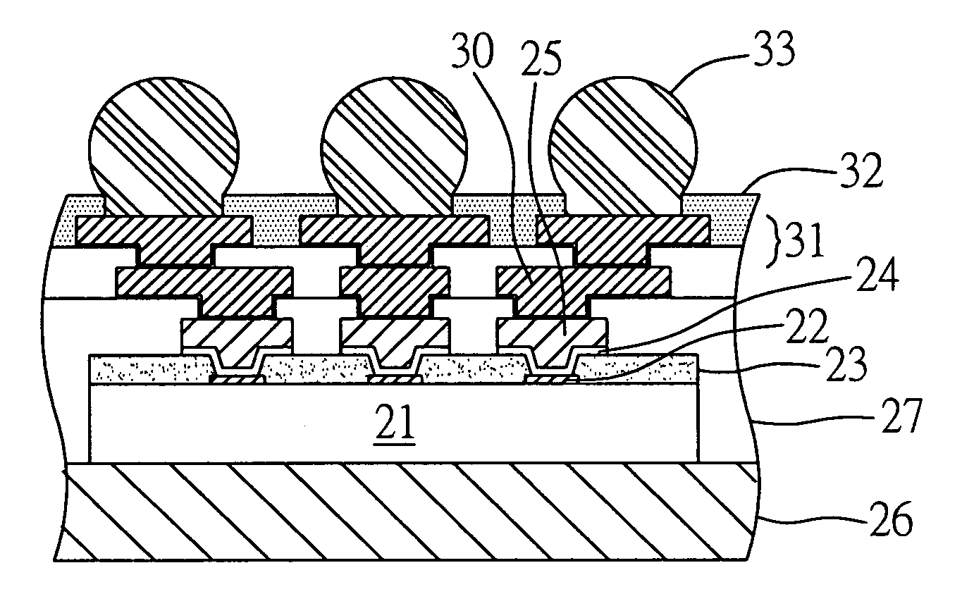
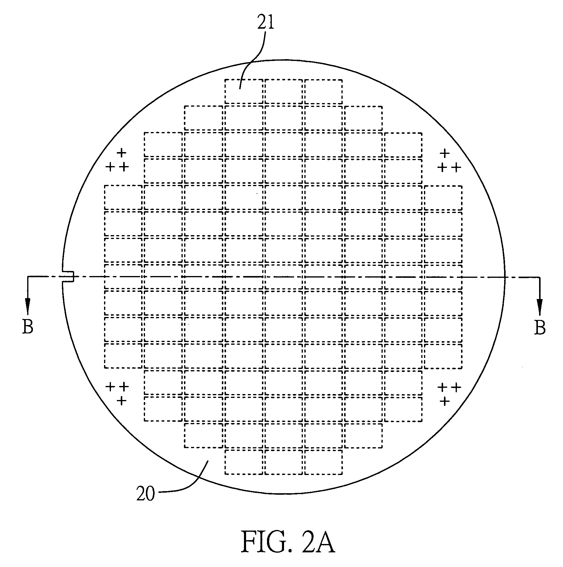
[0023]FIGS. 2A to 2I are cross-sectional views showing a method of fabricating a semiconductor electrical connection structure according to the present invention, wherein FIG. 2A is a top view of a semiconductor wafer, and FIGS. 2B to 2I are cross-sectional views showing a method of fabricating a build-up structure on a semiconductor chip according to a preferable embodiment of the present invention. It should be noted that the drawings are simplified schematic diagrams showing basic architecture of the present invention, and thus only show components or elements relevant to the present invention. The components or elements shown in the drawings are not made in real number, shape and size ratio. In practice, the number, shape and size ratio of components or elements can be flexibly arranged as an option of design, and the layout of components or elements would be more complex.

[0024] Referring first to FIG. 2A, a wafer 20 is provided comprising a plurality of semiconductor chips 21....


PUM


Abstract

A semiconductor electrical connection structure and a method of fabricating the same are provided. A wafer formed with a plurality of gold bumps thereon is divided into a plurality of individual chips. A carrier is prepared, and at least one of the chips is mounted on the carrier via a non-active surface of the chip. An insulating layer is applied on the carrier mounted with the chip, and formed with a plurality of openings using a laser drilling, photo imaging or plasma etching technique to expose the gold bumps via the openings. A conductive layer is formed on the insulating layer and in the openings. A pattered resist layer is applied on the conductive layer to define openings for electroplating. A circuit structure is electroplated in the openings of the resist layer so as to allow the chip to be electrically connected to an external device via the circuit structure.

Description

FIELD OF THE INVENTION [0001] The present invention relates to semiconductor electrical connection structures and methods of fabricating the same, and more particularly, to a semiconductor electrical connection structure and a fabrication method thereof without using a wire-bonding or flip-chip technique. BACKGROUND OF THE INVENTION [0002] Since the IBM Company has introduced a flip-chip packaging technique in early 1960s, as compared with a wire-bonding technique, the flip-chip technology is characterized in electrically connecting a semiconductor chip to a substrate by means of solder bumps instead of gold wires. Such flip-chip technology yields advantages that the packaging density can be increased to reduce the size of package, and electrical performance of the package can be improved as not requiring long metal or gold wires. Therefore, the industry has utilized high-temperature solder for electrically connecting a flip chip to a ceramic substrate by so-called control-collapse ...

Claims


Application Information

Patent Timeline
IPC IPC(8): H01L21/50H01L21/60H01L23/31
CPCH01L23/3114H01L24/11H01L24/12H01L2223/54493H01L2224/13099H01L2224/24011H01L2224/2402H01L2224/24226H01L2224/24227H01L2224/82039H01L2924/01016H01L2924/01022H01L2924/01029H01L2924/01046H01L2924/01074H01L2924/01078H01L2924/01079H01L2924/01082H01L2924/14H01L2924/15311H01L2924/01005H01L2924/01006H01L2924/01024H01L2924/01033H01L2924/014H01L2224/16225H01L2224/32225H01L2224/73204H01L2924/00H01L2924/10253H01L24/19H01L2224/023H01L2224/05001H01L2224/05022H01L2224/05572H01L2224/056H01L2924/00014H01L2924/15787H01L2924/351H01L2224/05099H01L2924/0001
Inventor HSU, SHIH-PING
Owner PHOENIX PRECISION TECH CORP
Why Eureka
Try Eureka