

Producing method of wired circuit board
- Summary
- Abstract
- Description
- Claims
- Application Information
AI Technical Summary
Benefits of technology
Problems solved by technology
Method used
Image

Examples
example 1
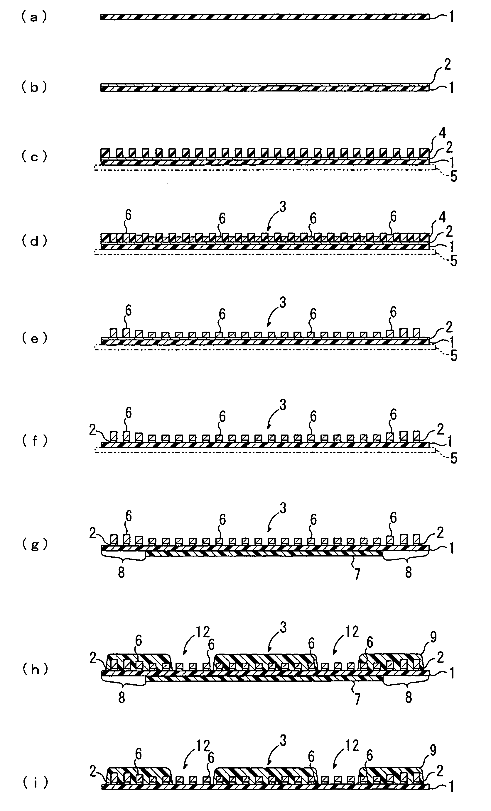
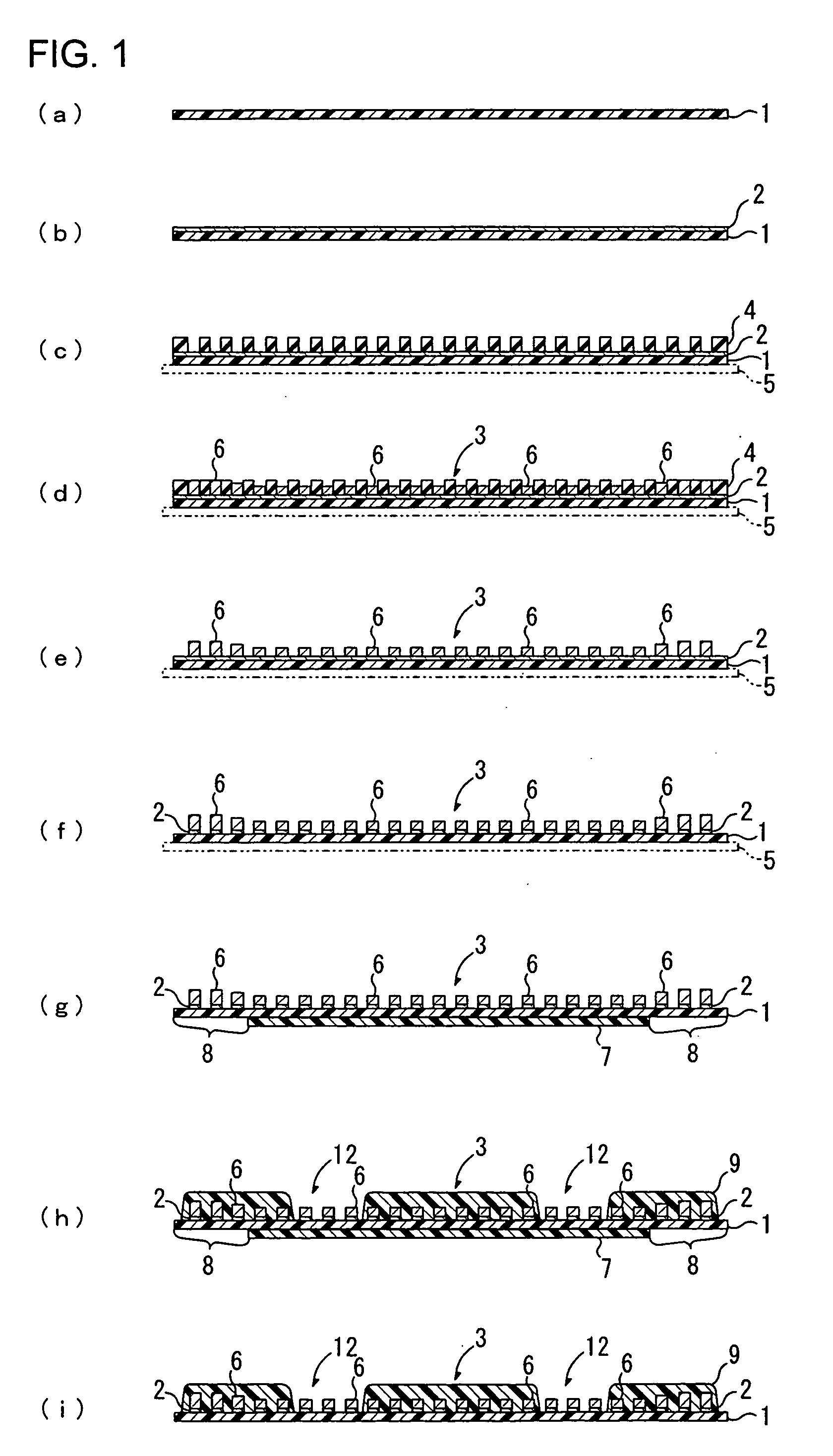
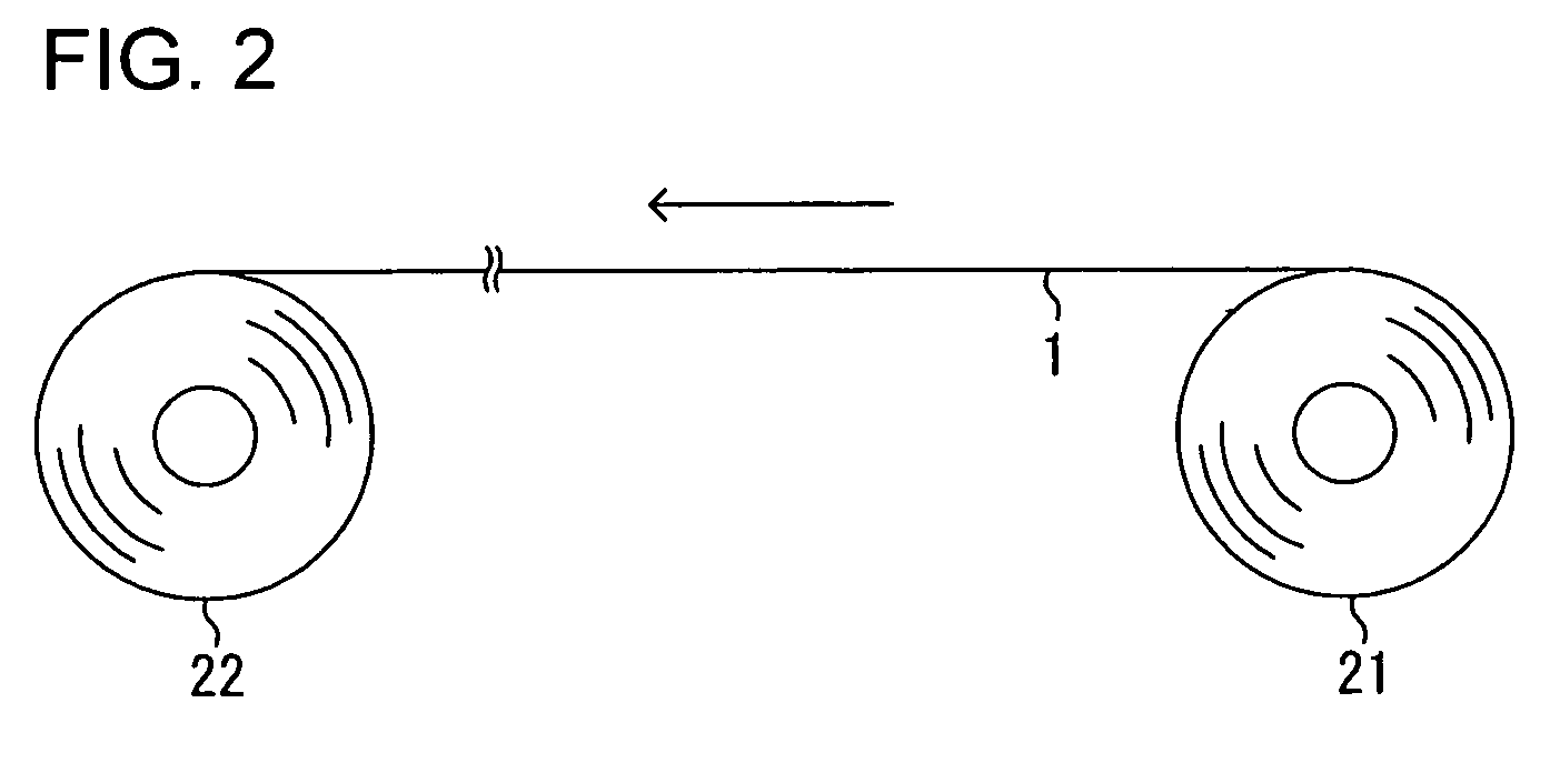
[0087] A flexible wired circuit board was produced by the roll-to-roll process having the following processes and using the manufacturing equipment.
[0088] An elongate base material of a polyimide film having a width of 250 mm and a thickness of 25 μm was prepared (Cf. FIG. 1(a)). Then, a thin metal film comprising a thin chromium film having a thickness of 30 nm and a thin copper film having a thickness of 200 nm was sequentially formed on the entire surface of the elongate base material by the sputtering process (Cf FIG. 1(b)).
[0089] Then, at the same time as the adhesive bonding of a photosensitive dry film resist having a thickness of 20 μm to a surface of the thin metal film, a wide stiffener sheet of polyethylene terephthalate film with adhesive having a width of 252 mm and a thickness of 50 μm was adhesively bonded to the back side of the elongate base material. Thereafter, the photosensitive dry film resist was exposed to light and developed, to form a plating resist in a r...
PUM
 Abstract
Description
Claims
Application Information