Semiconductor light emitting element and fabrication method thereof

a technology of semiconductors and light emitting elements, applied in the direction of semiconductor devices, basic electric elements, electrical devices, etc., can solve the problems of difficult dispersion, repeatability, low light extraction efficiency, etc., and achieve the effect of improving light extraction efficiency

Inactive Publication Date: 2006-04-13
SANKEN ELECTRIC CO LTD
View PDF12 Cites 29 Cited by
  • Summary
  • Abstract
  • Description
  • Claims
  • Application Information

AI Technical Summary

Benefits of technology

[0010] The present invention was made in view of the above-described circumstance, and it is an object of the present invention to provide a semiconductor light emitting element which can improve the light extraction efficiency, and a fabrication method thereof.

Problems solved by technology

Since the difference in the refraction index between the surface layer and the outside world is relatively large, the light extraction efficiency is relatively low.
However, the formation of such a scattering layer and window layer has problems in the viewpoints of workability, repeatability, etc.
However, it is extremely difficult to carry out the dispersion with a good repeatability and fabricate light emitting elements having a high uniformity and a desired luminance at a high yield.
Moreover, if the window layer disclosed in U.S. Pat. No. 5,233,204 is grown thick by an epitaxial method, the crystal might be deteriorated.

Method used


Image

  • Semiconductor light emitting element and fabrication method thereof
  • Semiconductor light emitting element and fabrication method thereof
  • Semiconductor light emitting element and fabrication method thereof

Examples


Embodiment Construction

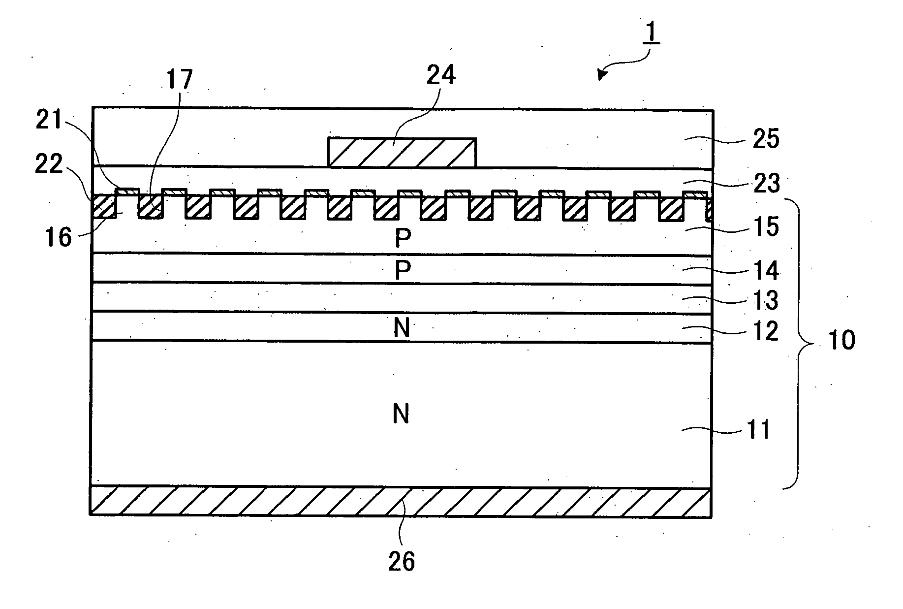
[0046] A semiconductor light emitting element and fabrication method thereof according to an embodiment of the present invention will now be explained with reference to the drawings, by illustrating a case where a light emitting diode is used as the light emitting element.

[0047] As shown in FIG. 1, a semiconductor light emitting element 1 according to the present embodiment comprises a semiconductor base 10, a contact electrode 21, a transparent dielectric film 22, a transparent conductor film 23, an anode electrode 24, a protection layer 25, and a cathode electrode 26. The semiconductor base 10 includes an N-type substrate 11, an N-type auxiliary layer 12, an active layer 13, a P-type auxiliary layer 14, and a window layer 15.

[0048] The N-type substrate 11 is formed of an N-type semiconductor substrate made of silicon (Si), gallium-arsenide (GaAs), gallium-phosphorus (GaP), silicon carbide (SiC), or the like. The N-type substrate 11 is formed with, for example, an impurity concen...


PUM


Abstract

In a semiconductor light emitting element, multiple bosses having a cylindrical shape and dispersed like islands, and recesses are formed on the upper surface of a window layer. A contact electrode is formed on the upper surface of the bosses. A transparent dielectric film is formed in the recesses. A transparent conductor film is formed on the transparent dielectric film and the contact electrode.

Description

BACKGROUND OF THE INVENTION [0001] 1. Field of the Invention [0002] The present invention relates to a semiconductor light emitting element such as a light emitting diode, a semiconductor laser, etc. and a fabrication method thereof. [0003] 2. Description of the Related Art [0004] To improve the luminance of a semiconductor light emitting element such as a light emitting diode, a semiconductor laser, etc., it is extremely important to efficiently extract the light emitted by the active layer of the light emitting element to the outside of the element. That is, it is necessary to restrict light reflection on the surface of the light emitting element as much as possible to let out the emitted light to the outside of the element and increase the so-called light extraction efficiency. [0005] As a means for restricting light reflection on the surface of the light emitting element and increasing the light extraction efficiency, there is a method for restricting total reflection on the sur...

Claims


Application Information

Patent Timeline
Patent Type & Authority Applications(United States)
IPC IPC(8): H01L33/00H01L33/14H01L33/22H01L33/30H01L33/38H01L33/42H01L33/44
CPCH01L33/22H01L33/30H01L33/387H01L33/42H01L2933/0016
Inventor MUROFUSHI, HITOSHITAKEDA, SHIRO
Owner SANKEN ELECTRIC CO LTD
Why Eureka
Try Eureka