Method for fabricating electrical connection structure of circuit board

Active Publication Date: 2006-04-13
PHOENIX PRECISION TECH CORP
View PDF2 Cites 26 Cited by
  • Summary
  • Abstract
  • Description
  • Claims
  • Application Information

AI Technical Summary

Benefits of technology

[0010] Still another objective of the present invention is to provide a method for fabricating an electrical connection structure of a circuit board, by which conductive materials are firstly formed on conductive pads of the circuit board, such that the conductive materials can be effectively fixed by a protective layer that is subsequently formed on the circuit board so as to increase the bonding strength of the conductive materials.
[0011] A further objective of the present invention is to provide a method for fabricating an electrical connection structure of a circuit board, which can prevent reduction in size of exposed conductive pads due to a protective layer formed on a surface of the circuit board and avoid an alignment problem during depositing a solder material by the conventional stencil printing technology.
[0012] A further objective of the present invention is to provide a method for fabricating an electrical connection structure of a circuit board, which can eliminate drawbacks in the conventional technology, such as difficulty in fabricating a stencil, increase in the fabrication costs of the stencil, and difficulty in passing a solder material through small grids of the stencil, due to the grids of the stencil being reduced in size according to a reduced size and a reduced pitch of conductive pads in the conventional stencil printing technology.
[0013] A further objective of the present invention is to provide a method for fabricating an electrical connection structure of a circuit board, which can solve problems of cleaning a stencil after a certain period of time of usage thereof and degradation of convenience and reliability in fabrication caused in the conventional stencil printing technology by residues of a solder material on walls of grids of the stencil being increased along with the times of printing being performed.
[0014] In accordance with the above and other objectives, the present invention proposes a method for fabricating an electrical connection structure of a circuit board, which comprises the steps of: providing a circuit board having a circuit layer, applying an insulating layer on a surface of the circuit board wherein the insulating layer is formed with a plurality of openings for exposing portions of the circuit layer thereon, forming a conductive layer on a surface of the insulating layer and in the openings of the insulating layer, and applying a patterned first resist layer on the conductive layer to expose portions of the conductive layer, so as to form a plurality of conductive pads and conductive circuits on the conductive layer by an electroplating process and allow the conductive pads to be connected to the portions of the circuit layer; applying a second resist layer on the circuit board and forming a plurality of openings in the second resist layer to expose the conductive pads; successively forming a first conductive material and a second conductive material on each of the conductive pads by the electroplating process; removing the first and second resist layers and a part of the conductive layer covered by the first resist layer on the circuit board; forming a protective layer on the surface of the circuit board to cover the first and second conductive materials on each of the conductive pads; and thinning the protective layer to expose the second conductive material corresponding in position to each of the conductive pads. In the present invention, the conductive layer and the patterned resist layer are firstly formed on the surface of the circuit board dur

Problems solved by technology

This thus causes an alignment problem during subsequent formation of solder bumps on the exposed conductive pads using the stencil printing technology.
Moreover, in consideration of the occupied space and the height of the protective layer, the size of grids or openings of the stencil should be accordingly decreased, thereby making fabrication of such stencil become difficult and also increasing the fabrication costs of the stencil.
This may further make the solder material hard to pass through the small grids of the stencil and lead to difficulty in fabrication.
Therefore, the stencil

Method used


Image

  • Method for fabricating electrical connection structure of circuit board
  • Method for fabricating electrical connection structure of circuit board
  • Method for fabricating electrical connection structure of circuit board

Examples


Embodiment Construction

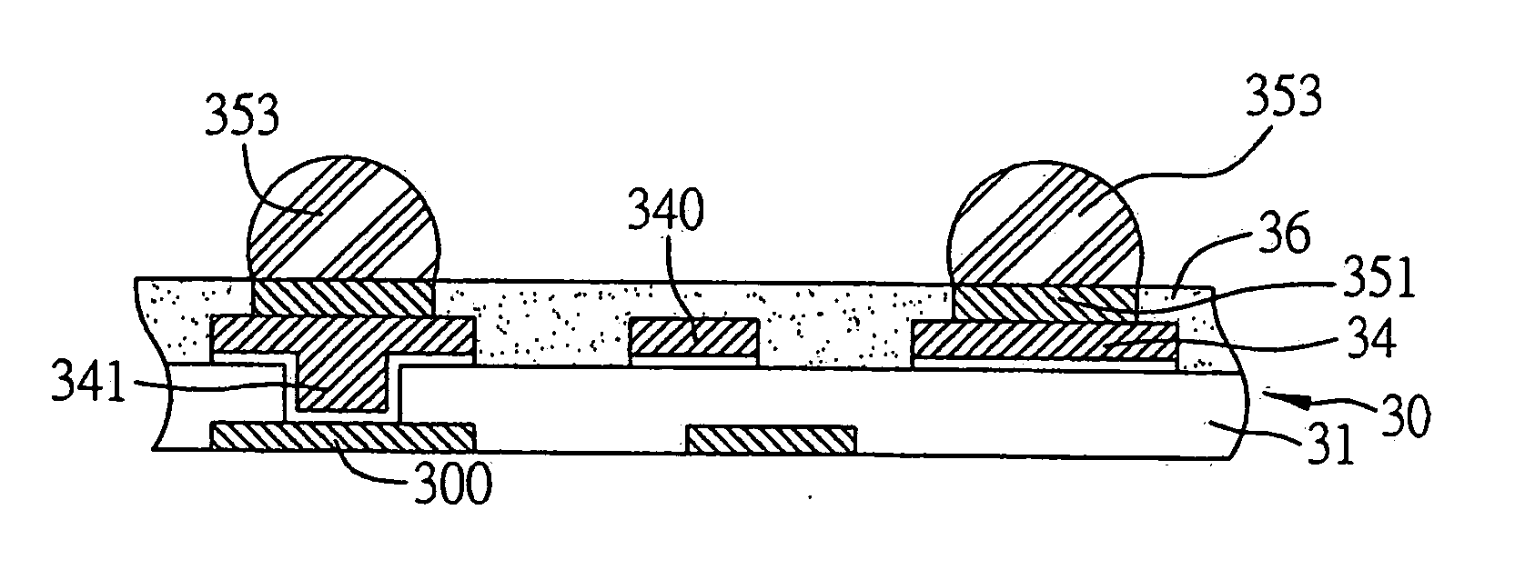
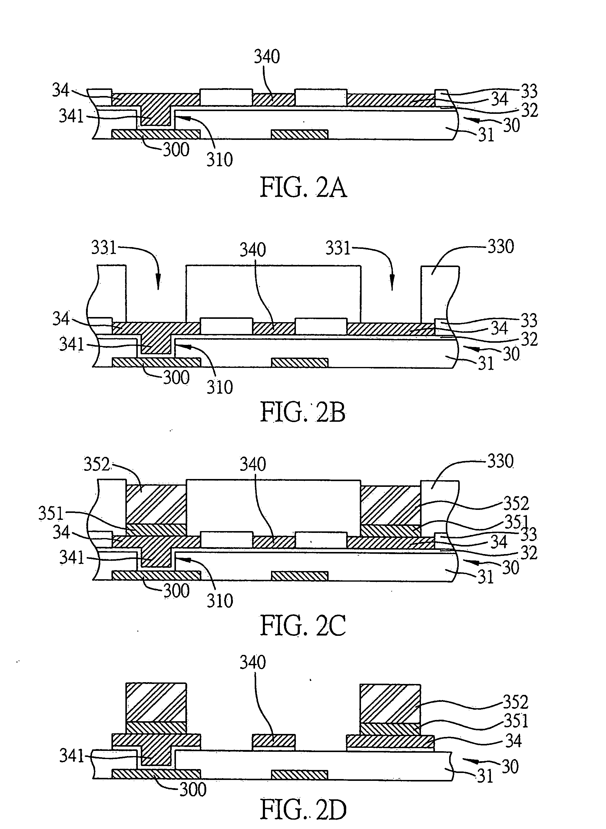
[0019]FIGS. 2A to 2G show a method for fabricating an electrical connection structure of a circuit board according to a preferred embodiment of the present invention.

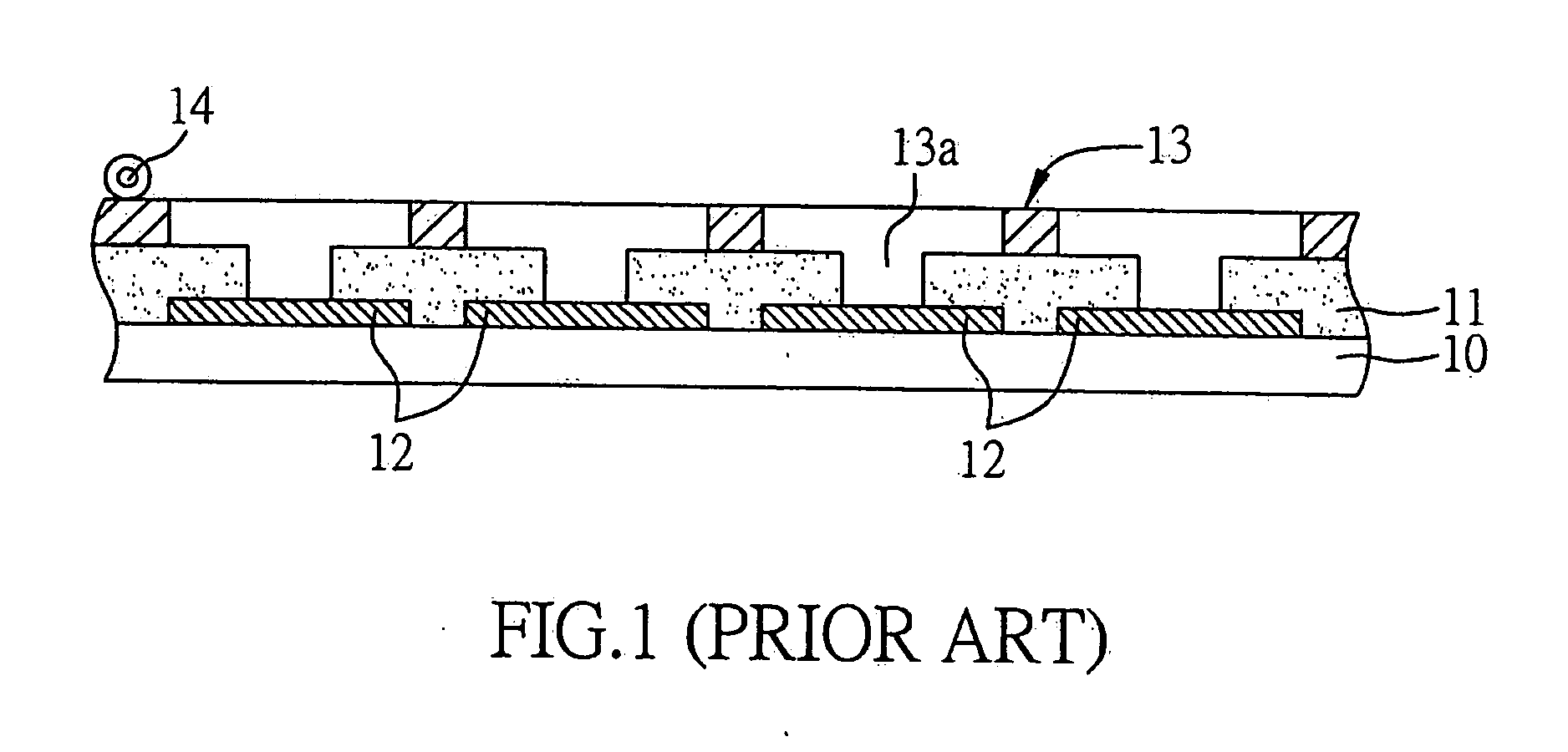
[0020] Referring to FIG. 2A, during a surface circuit forming process of a circuit board 30 having a circuit layer 300 thereon, a plurality of openings 310 are formed in an insulating layer 31 applied on a surface of the circuit board 30 to expose portions of the circuit layer 300, wherein the portions of the circuit layer 300 serve as connection lands for electrically interconnecting other circuit layers. It is to be understood that FIG. 2A to FIG. 2G only show the circuit layer 300 formed on the surface of the circuit board 30. In reality the circuit board 30 comprises the other interconnected circuit layers thereunder (not showen in the figs). Then, a conductive layer 32 is formed on a surface of the insulating layer 31 and in the openings 310, and is partly connected to the portions of the circuit layer 300 of the ...


PUM


Abstract

A method for fabricating an electrical connection structure of a circuit board is proposed. A patterned resist layer is formed on the circuit board having a plurality of conductive pads, and a plurality of openings is formed in the resist layer to expose the conductive pads. A first conductive material and a second conductive material are successively deposited in the openings of the resist layer and on each of the conductive pads. Then, the resist layer is removed. Subsequently, a protective layer is applied on the circuit board and covers the first and second conductive materials formed on each of the conductive pads. Finally, the protective layer is thinned to expose the second conductive material corresponding in position to each of the conductive pads. Thus, the circuit board can be electrically connected to an external device via the second conductive material.

Description

FIELD OF THE INVENTION [0001] The present invention relates to methods for fabricating electrical connection structures of circuit boards, and more particularly, to a method for fabricating conductive elements on conductive pads of a circuit board by an electroplating process. BACKGROUND OF THE INVENTION [0002] In the current flip-chip technology, electrode pads are formed on a surface of a semiconductor integrated circuit (IC) chip and corresponding conductive pads are formed on an organic package substrate, such that solder bumps or other conductive adhesive materials can be bonded between the electrode pads of the chip and the conductive pads of the package substrate so as to allow an active surface of the chip to be mounted on the package substrate in a face-down manner. The solder bumps or other conductive adhesive materials are used to provide electrically input / output connections and mechanical connections between the chip and the package substrate. [0003] After a subsequent ...

Claims


Application Information

Patent Timeline
IPC IPC(8): H01L21/4763
CPCH05K3/108H05K3/243H05K3/3473H05K2201/0394H05K2201/09481H05K2201/09563H05K2203/0574H05K2203/0723
Inventor HSU, SHIH-PINGTANG, SAO-HSIASHIH, CHAO-WENWANG, YING-TUNGHU, WEN-HUNG
Owner PHOENIX PRECISION TECH CORP
Why Eureka
Try Eureka