Apparatus for exposing a substrate, photomask and modified illuminating system of the apparatus, and method of forming a pattern on a substrate using the apparatus

Inactive Publication Date: 2006-04-20
SAMSUNG ELECTRONICS CO LTD
View PDF8 Cites 215 Cited by
  • Summary
  • Abstract
  • Description
  • Claims
  • Application Information

AI Technical Summary

Benefits of technology

[0019] Another object of the present invention to provide a photo-mask that can transfer a sharp image of a line space pattern having a small critical dimension to a layer of photoresist.
[0020] Still another object of the present invention is to provide a photo-mask that can facilitate the forming of

Problems solved by technology

Moreover, the uniformity of the line width of the WPR pattern significantly affects the product yield; therefore, reducing the line width of the WPR without maintaining uniformity in the line width has no advantages.
The yield of the photolithography process is thus severely limited by the need to perform the above-described pr

Method used


Image

  • Apparatus for exposing a substrate, photomask and modified illuminating system of the apparatus, and method of forming a pattern on a substrate using the apparatus
  • Apparatus for exposing a substrate, photomask and modified illuminating system of the apparatus, and method of forming a pattern on a substrate using the apparatus
  • Apparatus for exposing a substrate, photomask and modified illuminating system of the apparatus, and method of forming a pattern on a substrate using the apparatus

Examples


Embodiment Construction

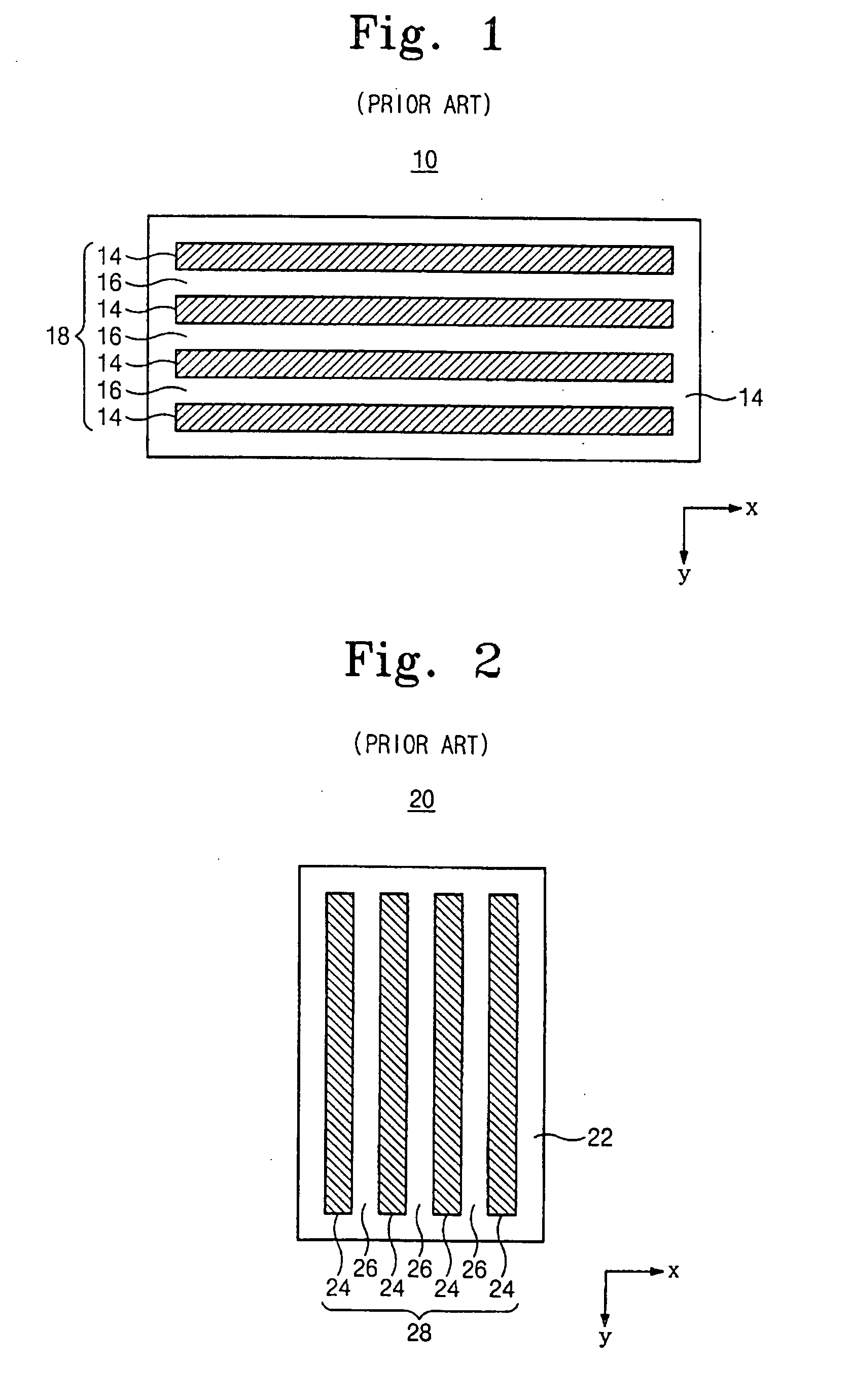
[0047] Referring to FIG. 7A, a photo-mask 70 according to the present invention includes a line / space pattern 78 oriented in a second direction (the direction of the Y axis) and a lattice pattern 79 oriented in a first direction (the direction of the X axis). The lines 74 of the line / space pattern 78 and the lattice pattern 79 are opaque and are formed on a transparent quartz substrate 72. The line / space pattern 78 consists of a series of parallel lines 74 extending in the second direction and spaces 76 defined between the lines 74. The lattice pattern 79 occupies the spaces 76 defined between the lines 74 of the line / space pattern 78 and consists of stripes extending perpendicular to the lines 74. The pitch P1 of the line / space pattern 78 is larger than the wavelength λ of the light emitted by the light source of the exposure apparatus for which the photo-mask 70 is designed. The pitch P2 of the lattice pattern 79 is smaller than the wavelength λ of the light source. Therefore, the...


PUM


Abstract

An exposure apparatus and photo-mask of the exposure apparatus can form a perpendicular line/space circuit pattern through only a single exposure process. The photo-mask includes a first line/space pattern oriented in a first direction, a second line/space pattern oriented in a second direction and lattice patterns, operating as polarizers, occupying the spaces of the line/space patterns. The exposure apparatus also includes a modified illuminating system. The modified illuminate system may be a composite polarization illuminating system having a shielding region, and a plurality of light transmission regions defined within the field of the shielding region. The light transmission regions are implemented as polarizers that polarize the light incident thereon in the first and second directions, respectively.

Description

BACKGROUND OF THE INVENTION [0001] The present invention relates to an exposure apparatus of photolithographic equipment used in the fabricating of a semiconductor device or the like. More particularly, the present invention relates to a photo-mask and an illuminating system of the exposure apparatus. [0002] The fabricating of an integrated circuit of a semiconductor device includes a photolithography process in which a pattern of a photo-mask is transcribed onto a wafer photoresist layer (WPR), i.e., a layer of photoresist coating a wafer. More specifically, the photo-mask is illuminated using a light source and an illuminating system to pick up an image of the pattern of the photo-mask. The pattern of the photo-mask corresponds to a circuit pattern that is to be formed on the wafer. [0003] A line / space circuit pattern is representative of the circuit patterns that are typically formed on a wafer. A photo-mask for use in forming such a line / space circuit pattern is illustrated in F...

Claims


Application Information

Patent Timeline
IPC IPC(8): G03B27/42G03C5/00G06F17/50G03F1/00G02B5/30G03F1/36G03F1/68G03F1/70H01L21/027
CPCG03F1/144G03F1/36G03F7/701G03F7/70125G03F7/70566G03F7/20
Inventor KIM, HO-CHUL
Owner SAMSUNG ELECTRONICS CO LTD
Why Eureka
Try Eureka