Thin film transistor, electro-optical device and electronic apparatus

a technology of electrooptical devices and thin film transistors, applied in the direction of electrical devices, semiconductor devices, instruments, etc., can solve the problems of high manufacturing cost, low productivity, and diffusion of atoms of layers, so as to improve the operational reliability, reduce the manufacturing cost, and prevent performance degradation and variation of characteristics of thin film transistors

Inactive Publication Date: 2006-04-27
SEIKO EPSON CORP
View PDF31 Cites 27 Cited by
  • Summary
  • Abstract
  • Description
  • Claims
  • Application Information

AI Technical Summary

Benefits of technology

[0009] A thin film transistor according to an aspect of the invention includes a semiconductor layer formed over a substrate, and an electrode member formed over the substrate by a liquid phase method. The electrode member includes a base layer composed of a metal material and an outer surface layer deposited on at least one surface of the base layer. The outer surface layer is formed of a metal material that is less susceptible to being dissolved in silicon and a silicon compound compared with the metal material constituting the base layer.
[0010] According to the configuration of the aspect of the invention, the outer surface layer can prevent the material constituting the base layer from diffusing into the adjacent silicon or silicon compound layer. Thus, performance degradation and variation of characteristics of the thin film transistor can be prevented. Therefore, the present configuration can provide a thin film transistor that achieves lowering of manufacturing costs thereof due to the formation of the electrode member by using a liquid phase method, and the improvement of its operational reliability.
[0011] A thin film transistor according to another aspect of the invention includes a semiconductor layer formed over a substrate, and an electrode member formed over the substrate. The electrode member has a structure in which a barrier layer and a base layer are sequentially deposited on top of each other by using a liquid phase method. The barrier layer is composed of a metal material. The base layer is composed of a metal material. The metal material constituting the barrier layer is at least one metal material selected from Ni, Ti, W and Mn.
[0012] According to the configuration, the barrier layer formed as a l...

Problems solved by technology

Therefore, the photolithography involves disadvantages of high manufacturing costs and low productivity.
However, a process for applying this technique to fabrication of TFTs, which are composed of a multi-layer structure on a substrate, may cause problems.
Therefore, this heating may c...

Method used


Image

  • Thin film transistor, electro-optical device and electronic apparatus
  • Thin film transistor, electro-optical device and electronic apparatus
  • Thin film transistor, electro-optical device and electronic apparatus

Examples


Embodiment Construction

Liquid Crystal Display

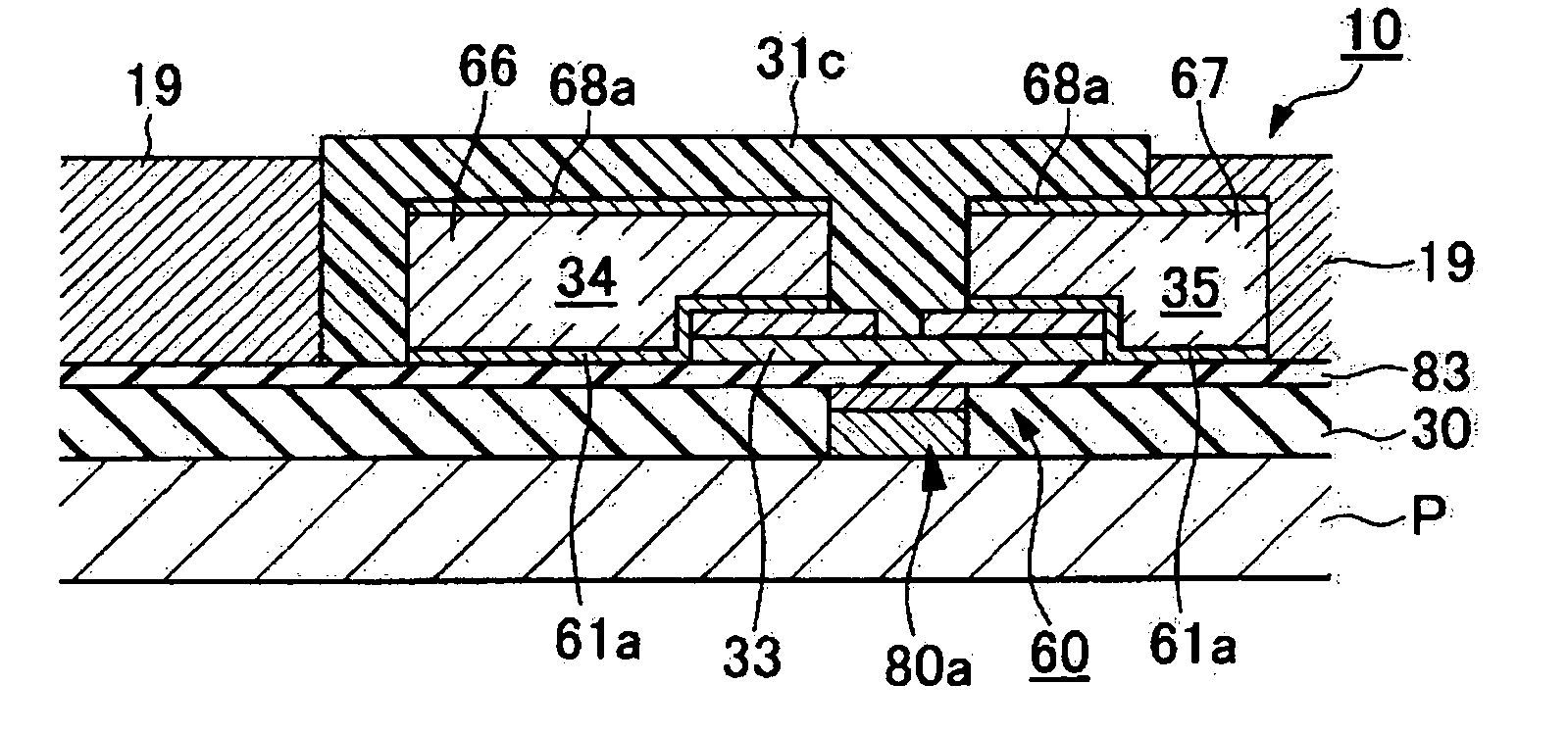
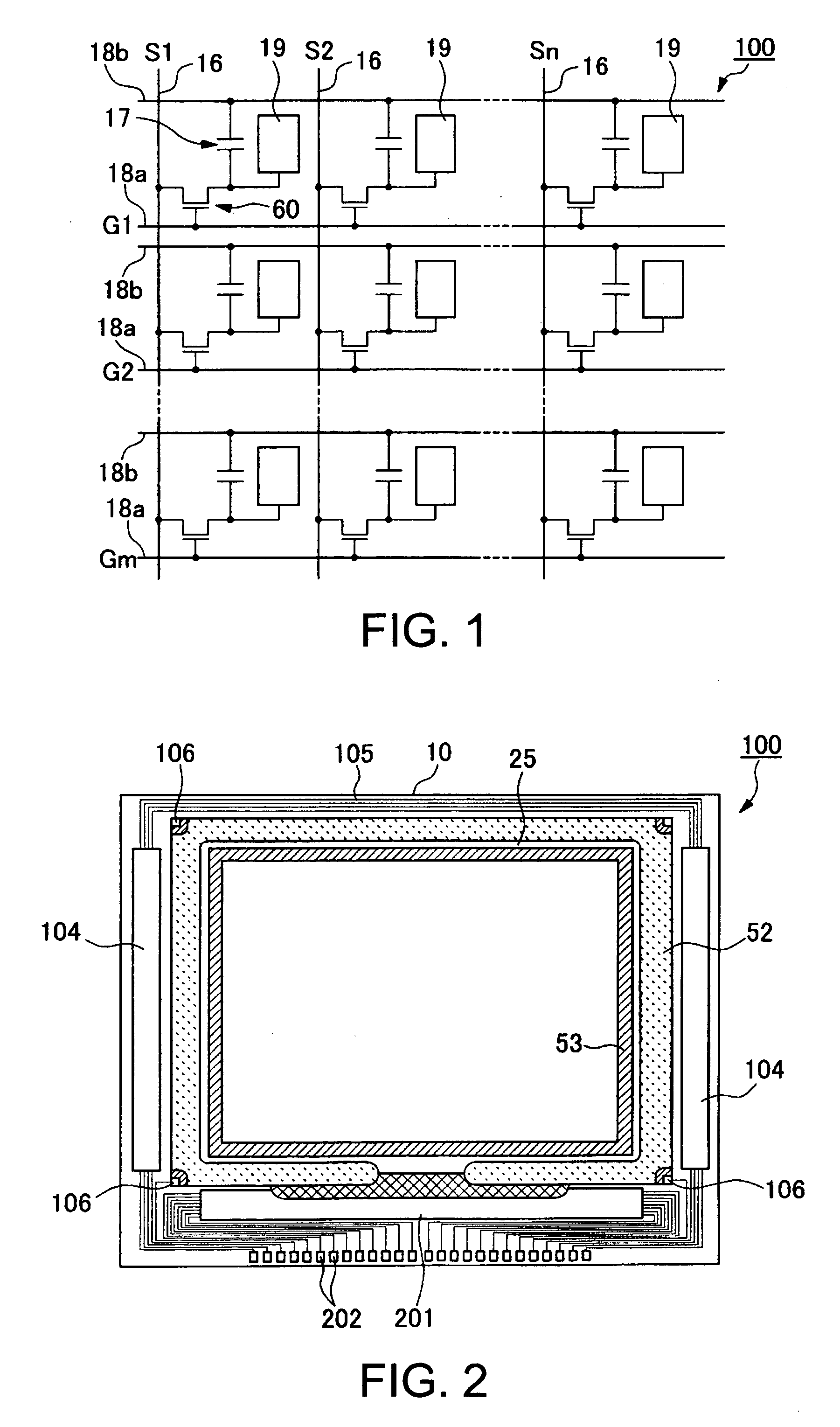
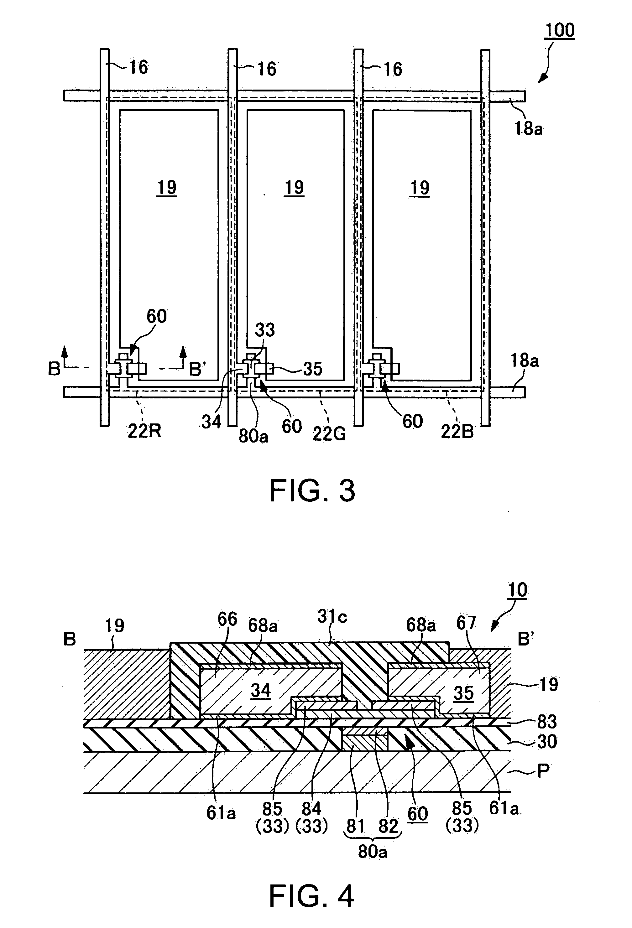
[0039]FIG. 1 is an equivalent circuit diagram illustrating a liquid crystal display 100 that is an electro-optical device according to one embodiment of the invention. The liquid crystal display 100 of the present embodiment includes a plurality of dots arranged in a matrix. Formed in each dot are a pixel electrode 19 and a TFT 60 that is a switching element for controlling the pixel electrode 19. A data line (electrode wire) 16 to which an image signal is supplied is electrically coupled to the source of the corresponding TFT 60. Image signals S1, S2, . . . , and Sn to be written to the data lines 16 are sequentially supplied in that order, or plural image signals of a respective one of signal groups are in turn supplied to the corresponding plural data lines 16 adjacent to each other. Furthermore, scan lines (electrode wires) 18a are electrically coupled to the gates of the TFTs 60, and scan signals G1, G2, . . . , and Gm are pulsatively and line-sequential...


PUM


Abstract

A thin film transistor includes a semiconductor layer formed over a substrate, and an electrode member formed over the substrate by a liquid phase method. The electrode member includes a base layer composed of a metal material and an outer surface layer deposited on at least one surface of the base layer. The outer surface layer is formed of a metal material that is less susceptible to being dissolved in silicon and a silicon compound compared with the metal material constituting the base layer.

Description

[0001] This application claims the benefit of Japanese Patent Applications No. 2004-306607 filed Oct. 21, 2004, No. 2004-306608 filed Oct. 21, 2004 and No. 2005-187724 filed Jun. 28, 2005. The entire disclosure of the prior applications are hereby incorporated by reference herein their entirety. BACKGROUND OF THE INVENTION [0002] 1. Technical Field [0003] The present invention relates to a thin film transistor, an electro-optical device and an electronic apparatus. [0004] 2. Related Art [0005] When manufacturing thin film transistors (TFTs), which are switching elements used in electro-optical devices such as liquid crystal devices, a photolithography method is used in steps of forming electrodes, wires or the like. The photolithography method is to form patterns of electrodes or wires composed of functional thin films through the following steps: a step of forming a blanket thin film by a film deposition method such as sputtering, plating or CVD, a step of applying a photosensitive...

Claims


Application Information

Patent Timeline
IPC IPC(8): H01L27/12H01L27/01
CPCH01L27/12H01L27/1292H01L29/4908H01L29/458G02F1/136
Inventor KOBAYASHI, YOSUKE
Owner SEIKO EPSON CORP
Why Eureka
Try Eureka