Early detection of metal wiring reliability using a noise spectrum

a technology of noise spectrum and metal wiring, applied in the direction of individual semiconductor device testing, semiconductor/solid-state device testing/measurement, instruments, etc., can solve the problems of void formation, defects in the fabrication of integrated circuits,

Inactive Publication Date: 2006-04-27
APPLIED MATERIALS INC
View PDF13 Cites 13 Cited by
  • Summary
  • Abstract
  • Description
  • Claims
  • Application Information

AI Technical Summary

Benefits of technology

[0009] Embodiments of the invention generally provide a method and apparatus for inspecting a substrate in a substrate processing system. In one embodiment, a method for determining the reliability of one or more features having one or more metal materials formed on a substrate includes placing the substrate in a substrate processing system, measuring a noise spectrum of a process variable affecting the processing of the substrate while the substrate is inside the substrate processing system, comparing the noise spectrum of the process variable for the one or more features having the one or more metal materials thereon to a reference noise spectrum, and determining the reliability of the one or more features on the substrate. The process variable may include a bias applied to the substrate, a plasma applied to the substrate processing system, a current applied to the substrate processing system, an electroplating current, etc., such as a plasma current, a plasma voltage, a plasma bias current, a plating current, among others.
[0010] In another embodiment, a method for determining the reliability of one or more copper wire features formed on a substrate is provided. The method includes measuring a noise spectrum of the one or more copper wire features after the substrate is processed by a substrate processing system and before the substrate is packaged into integrated circuit devices, comparing the noise spectrum of the one or more copper wire features to a reference noise spectrum, and determining the reliability of the one or more copper wire features on the substrate.
[0011] In still another embodiment, a method for determining the reliability of one or more features having one or more metal materials formed on a substrate includes placing the substrate in an electroplating processing system, measuring an electroplating current spectrum of the one or more features while the substrate is inside the electroplating processing system, comparing the electroplating current spectrum of the one or more features having the one or more metal materials thereon to a reference electroplating current spectrum, and determining the reliability of the one or more features on the substrate.
[0012] Another embodiment of the invention includes a semiconductor substrate processing system for processing a substrate. The semiconductor substrate processing system includes one or more substrate processing units adapted to process the substrate and form one or more features having one or more material layers thereon, and one or more substrate inspection units connected to the one or more substrate processing units and adapted to measure a noise spectrum of the one or more features and determine the reliability of the one or more features on the substrate. Further, the one or more substrate inspection units include one or more ammeters or one or more spectrum analyzers.
[0013] Yet another embodiment of the invention includes a computer-readable medium for determining the reliability of one or more features having one or more materials formed on a substrate, including instructions configured to control a substrate processing system, monitor the substrate processed by the substrate processing system, and perform one or more steps. In one aspect, the one or more steps include measuring a noise spectrum of a process variable affecting the processing of the substrate while the substrate is inside the substrate processing system, comparing the noise spectrum of the process variable for the one or more features to a reference noise spectrum, and determining the reliability of the one or more features on the substrate. In another aspect, the one or more steps include measuring a noise spectrum of the one or more features after the substrate is processed by the substrate processing system, comparing the noise spectrum of the one or more features having the one or more materials thereon to a reference noise spectrum, and determining the reliability of the one or more features on the substrate.

Problems solved by technology

Fabrication of integrated circuits (IC) having multiple levels of patterned metallization lines and interconnects which are separated from one another by interlayer dielectrics to form features, e.g., vias, trenches, holes, plugs, wires, lines, contacts, dies and, studs, etc., are prone to include defects thereon.
For example, electromigration along a metal conductor during metal wiring may cause thinning or thickening of the conductor resulting in void and hillock formation, respectively, as well as damage to metallization lines and interconnects.
However, the inspection equipment needed has become ever more complex and expensive.
However, these techniques are destructive to the features formed on a semiconductor substrate, time-consuming to perform, and thus may not be suitable during semiconductor manufacturing for defect detection.
These electromigration (EM) tests generally subject tested samples to relatively high stresses, such as forcing constant high current or high temperature to the tested samples, which are very destructive and are very time-consuming to perform, typically on the order of several hours to days or weeks, in order to predict a time that the tested samples will fail by extrapolating obtained information into years.
In addition, the unique structures utilized on wafer-level testing to evaluate the result of stress can also cause failure of the IC.
Further, the test structures occupy very small size between dies or vias which may have low defect density, thus are not sensitive enough to represent defect density prior to costly and time-consuming burn-in schedules of the integrated circuits.
Metal wiring reliability using a noise spectrum is generally limited to packaged ICs and has not yet been implemented during processing of thin film deposition or planarization prior to fabricating integrated circuits and packaging into integrated circuit devices.
Also, noise measurement on copper wire structures was not successful, partly due to the presence of interface void formation between materials of poor adhesion with each other on a small device active area.
In addition, direct application of electrical probes on the ever small semiconductor structures during manufacturing are prone to errors caused by background noise.
Therefore, there is a need for inspection of a semiconductor substrate while it is still inside a substrate processing system to look at reliability and quality of features formed on the semiconductor substrate before costly and time-consuming testing on fabricated and / or packaged integrated circuits.

Method used


Image

  • Early detection of metal wiring reliability using a noise spectrum
  • Early detection of metal wiring reliability using a noise spectrum
  • Early detection of metal wiring reliability using a noise spectrum

Examples


Embodiment Construction

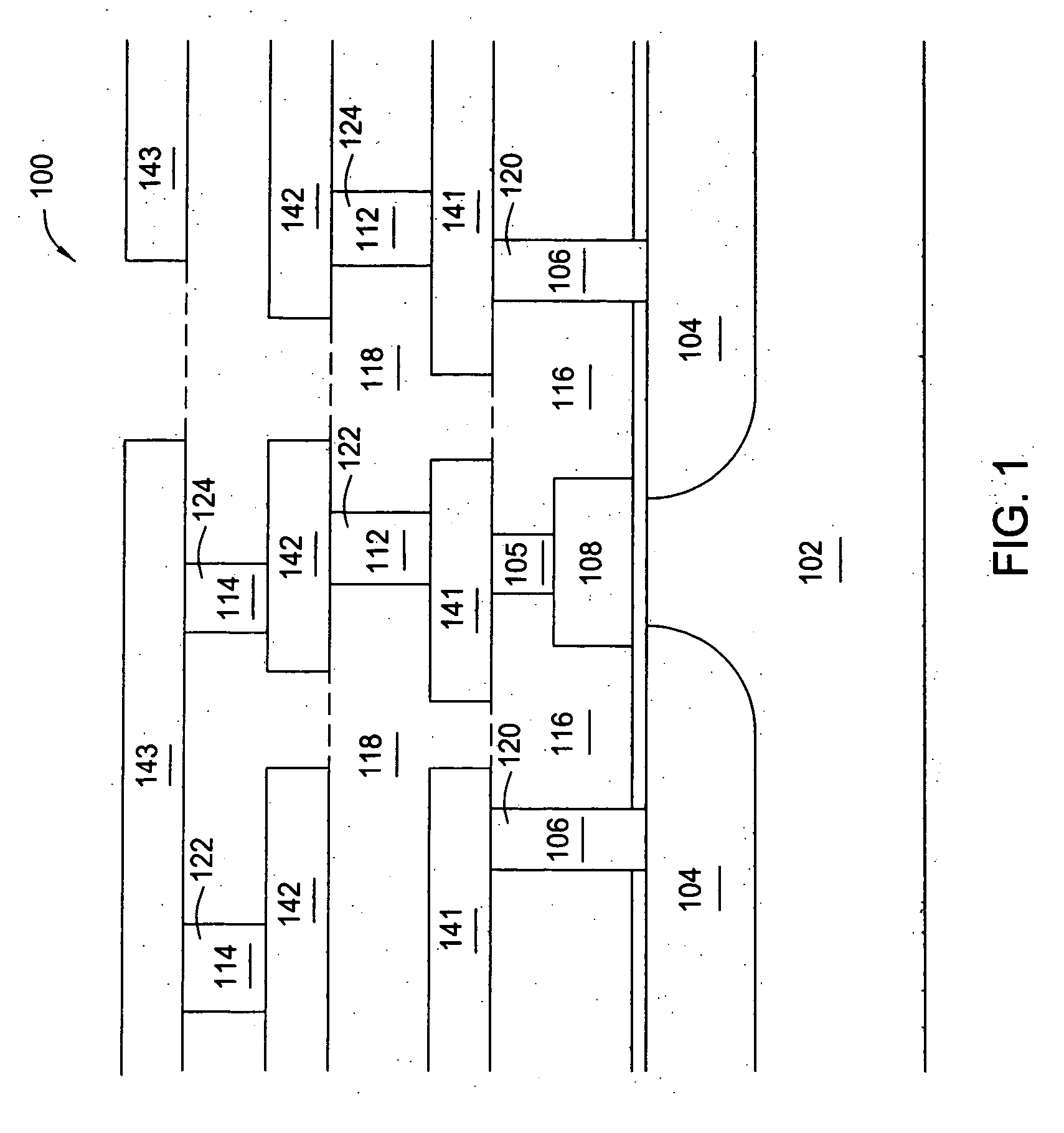
[0027] The present invention generally relates to a method and apparatus for monitoring and inspecting defects formed during processing of a semiconductor substrate by exploiting the quality of features formed on the semiconductor substrate at early time in order to predict reliability of the features which are later fabricated and packaged into integrated circuits or devices. Further, the reliability of various features on a substrate are predicted from a noise spectrum, at the time of deposition, sputtering, planarization, and / or processing the substrate, by a monitoring / inspection module coupled to a substrate processing system, such as at time zero of integrated circuits or devices, i.e., before forming and packaging into semiconductor integrated circuits or devices.

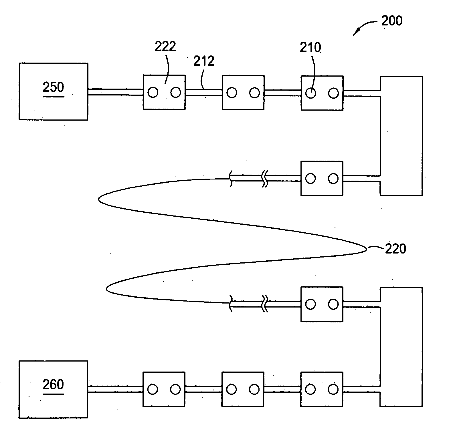
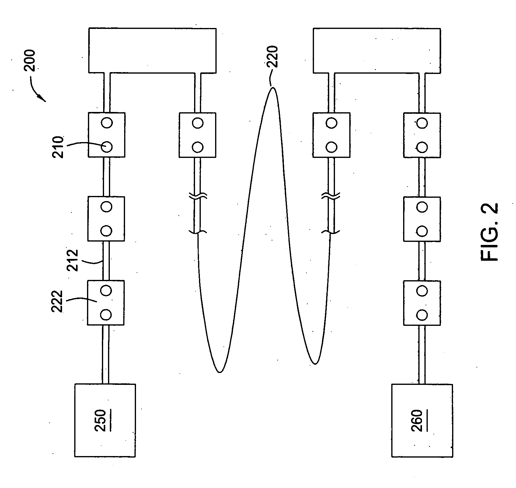
[0028] One aspect of the invention includes detection of reliability characteristics of a single level or multiple level metal interconnect semiconductor structure. The interconnect semiconductor structure can be fo...


PUM


Abstract

The present invention generally provides an apparatus and a method for inspecting a substrate in a substrate processing system. In one aspect, a voltage or current source is used in conjunction with a power density receiving device, such as a spectrometer, to inspect a substrate for various noise spectrum signatures. In one embodiment, spectral data collected from a given substrate is used to generate a current or voltage spectral signature. This spectral signature may then be compared to a reference spectral density signature to predict reliability of a feature structure of a substrate in processing and feedback to the substrate processing system for substrate processing control. Embodiments of the invention further include computer-readable media containing instructions for controlling the substrate processing system, and computer program products having computer-readable program code embodied therein for controlling the substrate processing system and inspecting defects on semiconductor features.

Description

BACKGROUND OF THE INVENTION [0001] 1. Field of the Invention [0002] Embodiments of the present invention generally relate to a method and apparatus for reliable processing of a semiconductor substrate without any defects thereon. More particularly, this invention relates to inspection of a semiconductor substrate during manufacturing of high-density semiconductor devices with submicron features. [0003] 2. Description of the Related Art [0004] Current demands for high performance associated with very large scale integration (VLSI) and ultra large scale integration (ULSI) require smaller submicron feature sizes, faster speeds, denser components and improved reliability. Fabrication of integrated circuits (IC) having multiple levels of patterned metallization lines and interconnects which are separated from one another by interlayer dielectrics to form features, e.g., vias, trenches, holes, plugs, wires, lines, contacts, dies and, studs, etc., are prone to include defects thereon. For ...

Claims


Application Information

Patent Timeline
Patent Type & Authority Applications(United States)
IPC IPC(8): H01L21/66
CPCH01L22/12H01L22/34H01L2924/0002H01L2924/00
Inventor SMAYLING, MICHAEL C.YOST, DENNIS J.
Owner APPLIED MATERIALS INC
Why Eureka
Try Eureka