Ultraviolet laser ablative patterning of microstructures in semiconductors
Inactive Publication Date: 2006-05-04
BAIRD BRIAN W +5
View PDF52 Cites 47 Cited by
Summary
Abstract
Description
Claims
Application Information
AI Technical Summary
This helps you quickly interpret patents by identifying the three key elements:
Problems solved by technology
Method used
Benefits of technology
[0017] An advantage of using UV wavelengths is the capability of producing spot sizes significantly smaller than those achievable with longer wavelength sources. This small spot size capability enables the production of micron-scale feature sizes in silicon. Also, for a fixed spot size achievable with conventional Gaussian focusing techniques, a shorter wavelength allows for formation of features with improved aspect ratios due
Problems solved by technology
However, since silicon is a weak absorber at 1064 nm, significant problems have been encountered in laser dicing processes operating at or near this wavelength.
The cut quality is typically observed to be marred by redeposition of silicon along the wafer surface and along the walls of the cut.
This apparent redeposition of silicon made the holes unsuitable for further processing.
He teaches that the primary
Method used
Image
Click on the blue label to locate the original text in one second.
Reading with bidirectional positioning of images and text.
Examples
Embodiment Construction
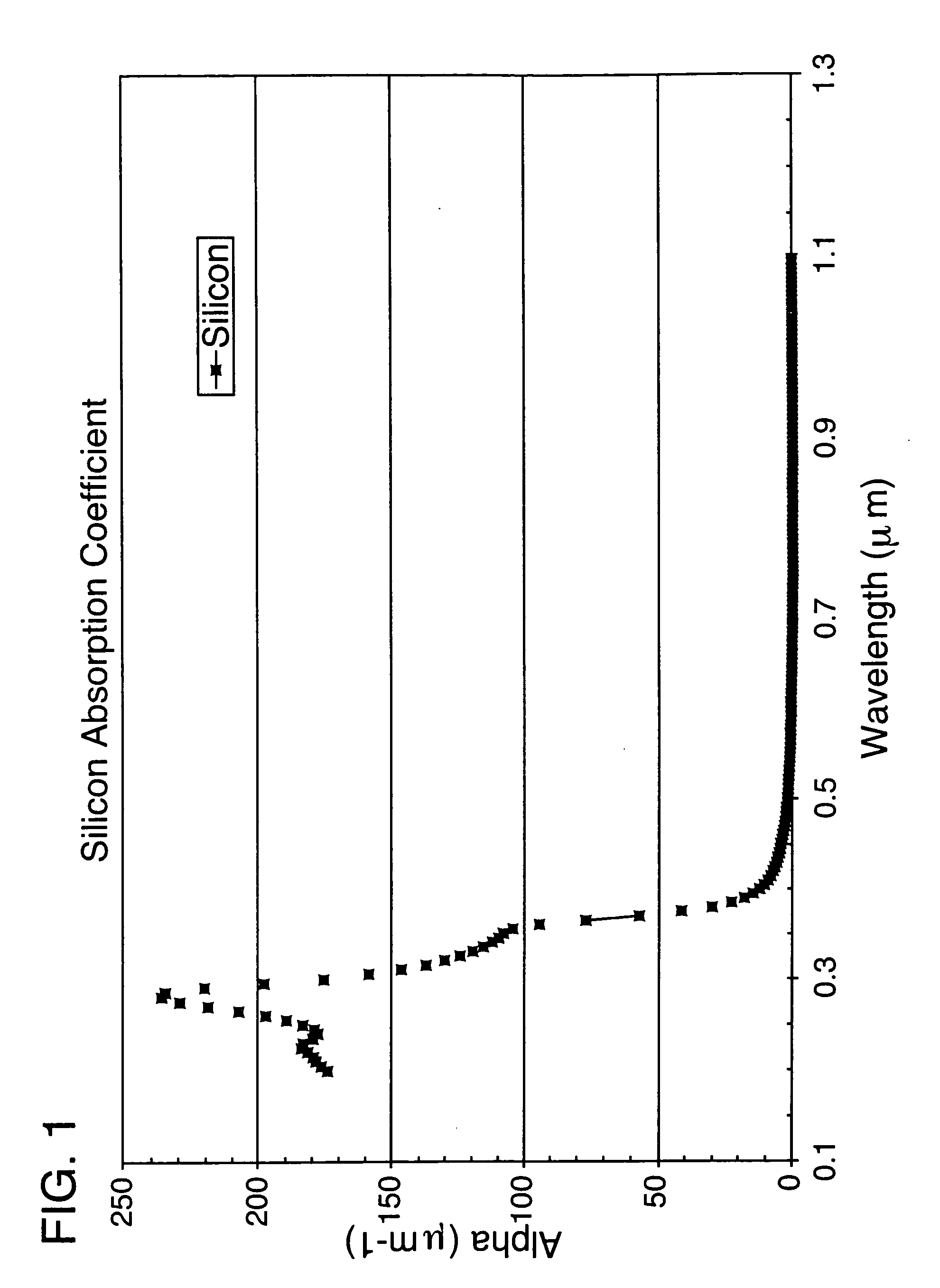
[0033]FIG. 1 displays the optical absorption coefficient of silicon as a function of wavelength. With reference to FIG. 1, silicon exhibits a very sharp rise in the optical absorption at wavelengths in the ultraviolet. The present invention advantageously utilizes laser wavelengths shorter than 390 nm and takes advantage of the increased absorption of silicon in the ultraviolet to efficiently ablate silicon and thereby form a variety of useful patterns or features directly in silicon. The absorption behavior facilitates strongly ablative removal of silicon in the ultraviolet with a greatly reduced thermally affected zone in comparison with features formed using either 532 nm or 1064 nm pulsed output as taught by the prior art.
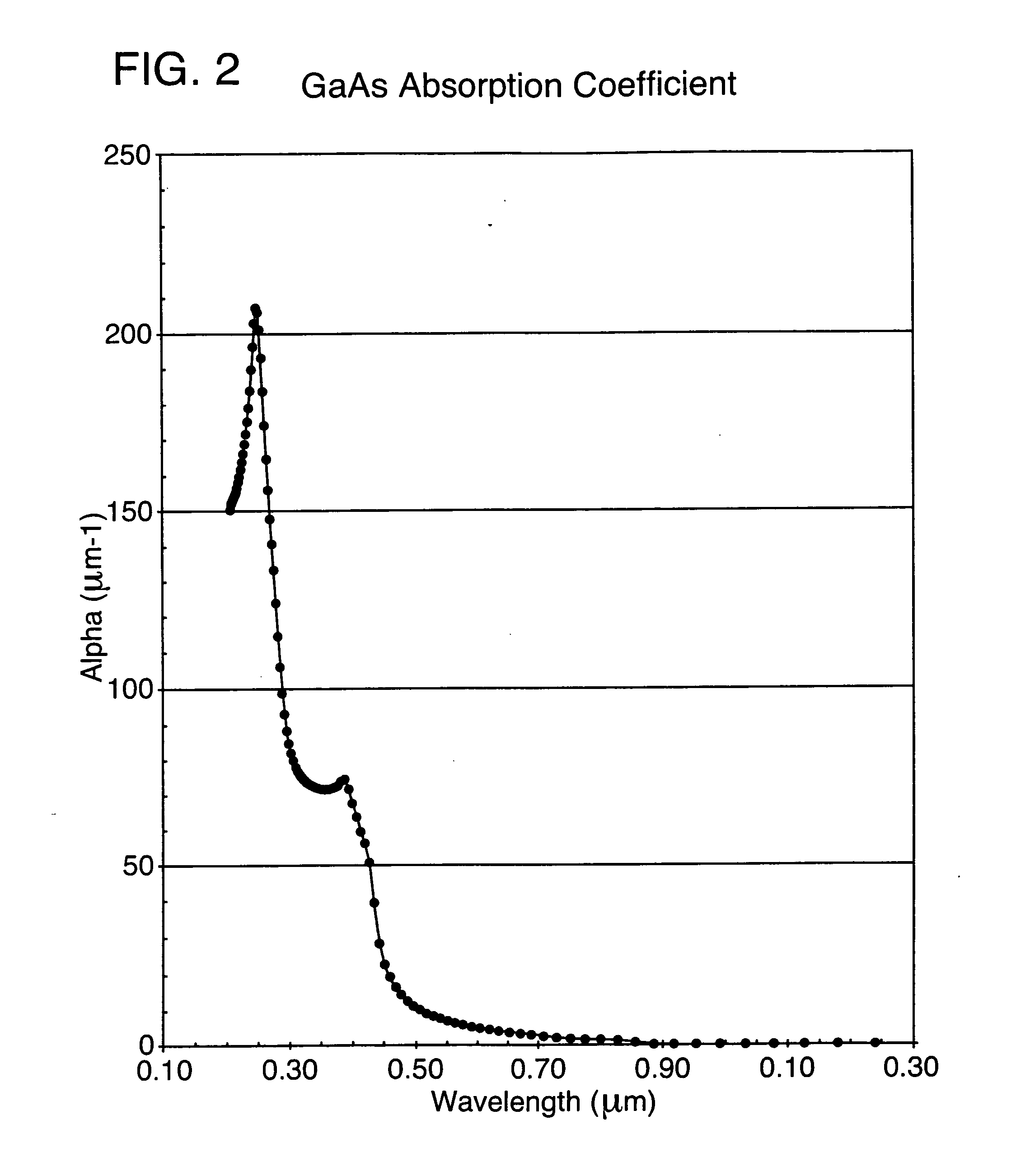
[0034]FIG. 2 displays the optical absorption coefficient of GaAs as a function of wavelength. With reference to FIG. 2, GaAs exhibits a very sharp rise in the optical absorption at wavelengths in the ultraviolet. The absorption coefficient at 355 nm of GaAs an...
PUM
Property
Measurement
Unit
Length
aaaaa
aaaaa
Length
aaaaa
aaaaa
Time
aaaaa
aaaaa
Abstract
Patterns with feature sizes of less than 50 microns are rapidly formed directly in semiconductors, particularly silicon, GaAs, indium phosphide, or single crystalline sapphire, using ultraviolet laser ablation. These patterns include very high aspect ratio cylindrical through-hole openings for integrated circuit connections; singulation of processed die contained on semiconductor wafers; and microtab cutting to separate microcircuit workpieces from a parent semiconductor wafer. Laser output pulses (32) from a diode-pumped, Q-switched frequency-tripled Nd:YAG, Nd:YVO4, or Nd:YLF is directed to the workpiece (12) with high speed precision using a compound beam positioner. The optical system produces a Gaussian spot size, or top hat beam profile, of about 10 microns. The pulse energy used for high-speed ablative processing of semiconductors using this focused spot size is greater than 200 μJ per pulse at pulse repetition frequencies greater than 5 kHz and preferably above 15 kHz. The laser pulsewidth measured at the full width half-maximum points is preferably less than 80 ns.
Description
RELATED APPLICATIONS [0001] This patent application which derives priority from U.S. Provisional Application No. 60 / 297,281, filed Jun. 8, 2001; from U.S. patent application Ser. No. 09 / 957,633, filed Sep. 19, 2001 (now abandoned), which claims priority from U.S. Provisional Application No. 60 / 233,914, filed Sep. 20, 2000; from U.S. patent application Ser. No. 10 / 017,497, filed Dec. 14, 2001, which claims priority from U.S. Provisional Application No. 60 / 265,556, filed Jan. 31, 2001; and from U.S. patent application Ser. No. 09 / 803,382, filed Mar. 9, 2001 (now abandoned), which claims priority from U.S. Provisional Application No. 60 / 233,913, filed Sep. 20, 2000.TECHNICAL FIELD [0002] This invention relates to a method and / or apparatus for high-speed formation of micron-scale features by ablation of semiconductors, and particularly silicon, using pulsed output of an ultraviolet (UV) laser. BACKGROUND OF THE INVENTION [0003] The semiconductor industry utilizes numerous techniques to ...
Claims
Application Information
Patent Timeline
Application Date:The date an application was filed.
Publication Date:The date a patent or application was officially published.
First Publication Date:The earliest publication date of a patent with the same application number.
Issue Date:Publication date of the patent grant document.
PCT Entry Date:The Entry date of PCT National Phase.
Estimated Expiry Date:The statutory expiry date of a patent right according to the Patent Law, and it is the longest term of protection that the patent right can achieve without the termination of the patent right due to other reasons(Term extension factor has been taken into account ).
Invalid Date:Actual expiry date is based on effective date or publication date of legal transaction data of invalid patent.