

Liquid crystal display device and method of fabricating the same
a liquid crystal display and liquid crystal technology, applied in semiconductor devices, instruments, electrical devices, etc., can solve the problems of complex manufacturing process and high manufacturing cost, and achieve the effect of simplifying the manufacturing method and improving the aperture ratio
- Summary
- Abstract
- Description
- Claims
- Application Information
AI Technical Summary
Benefits of technology
Problems solved by technology
Method used
Image

Examples
first embodiment
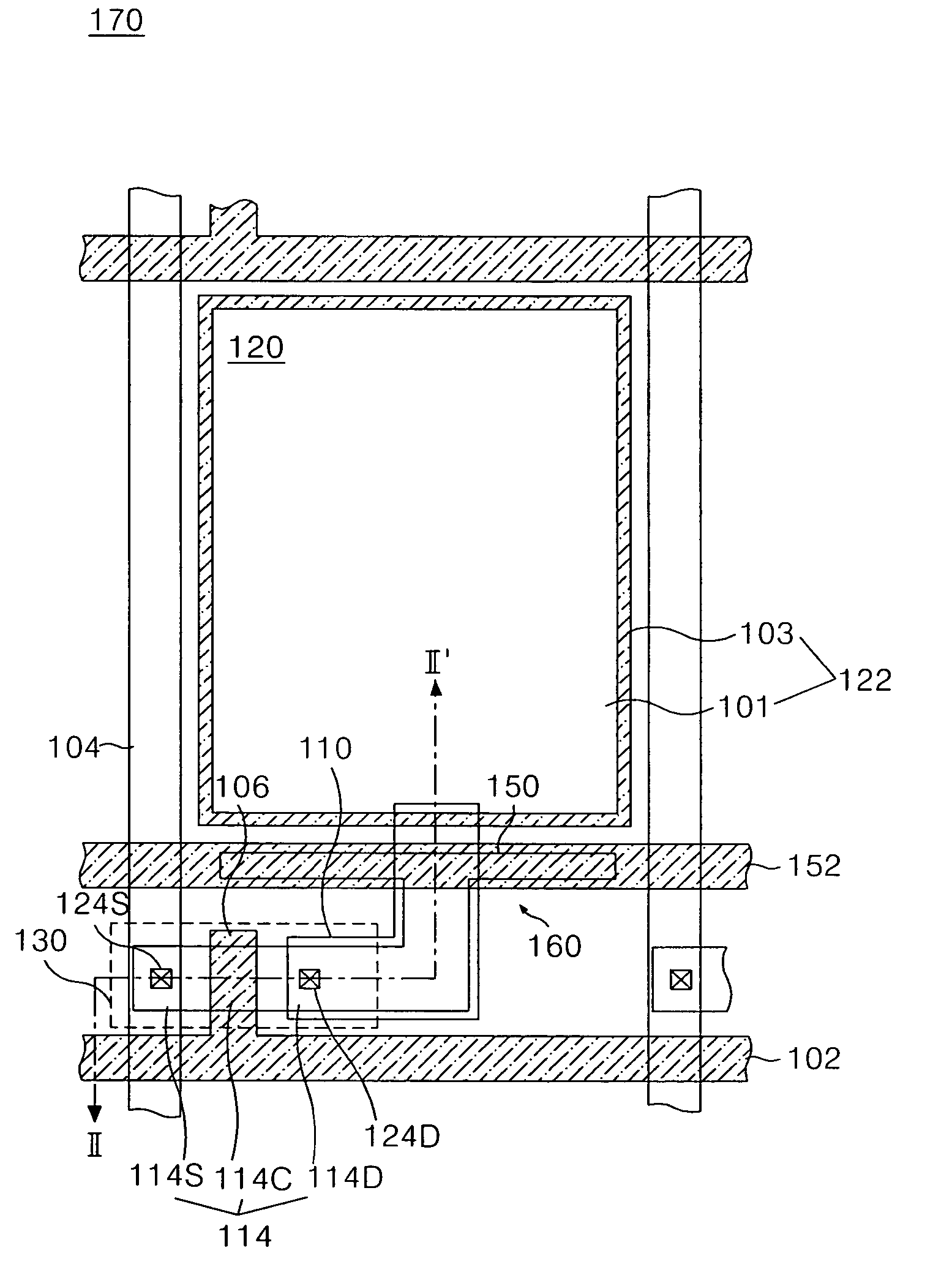
[0043]FIG. 4 is a plan view illustrating a portion of a thin film transistor substrate of a poly-silicon liquid crystal display device according to the present invention, and FIG. 5 is a cross-sectional view of the thin film transistor substrate taken along the line II-II′ in FIG. 4.
[0044] Referring to FIGS. 4 and 5, the thin film transistor (TFT) substrate 170 includes a gate line 102 and a data line 104, a TFT 130 connected to the gate line 102 and the data line 104, a pixel electrode 122 and a storage capacitor 160 connected to the TFT 130, and a storage line 152 connected to the storage capacitor 160. Although the TFT 130 can be either an NMOS-TFT or PMOS-TFT, the TFT 130 employing an NMOS-TFT will now be described.
[0045] The data line 104 crosses the gate line 102 and the storage line 152 with an interlayer insulating film 118 therebetween to define a pixel area provided with the pixel electrode 122.
[0046] The TFT 130 applies a video signal on the data line 104 to the pixel e...
second embodiment
[0078]FIGS. 11A and 11B are a plan view and a cross-sectional view, respectively, illustrating a second mask process in a method of fabricating the thin film transistor substrate according to the present invention.
[0079] Referring to FIGS. 11A and 11B, the gate insulating film 216 is formed on the buffer film 212 provided with the first and second active layers 214 and 250, and the pixel electrode 222, along with a double-layer structure of the gate line 202, the gate electrode 206 and the storage line 252, is formed thereon by the second mask process.
[0080] The gate insulating film 216 is provided by entirely depositing an inorganic insulating film such as SiO2, etc. onto the buffer film 212 provided with the first and second active layers 214 and 250. Then, the transparent conductive layer 201 and the metal layer 203 are deposited on the gate insulating film 216 by the sputtering, etc. The transparent conductive layer 201 is formed of indium-tin-oxide (ITO), tin-oxide (TO) or ind...
third embodiment
[0092]FIG. 15 is a plan view illustrating a poly-silicon liquid crystal display panel according to the present invention and an assembly process.
[0093] The poly-silicon liquid crystal display panel illustrated in FIG. 15 has the same elements as the poly-silicon liquid crystal display panel illustrated in FIG. 14, except that a black matrix 380 of a color filter substrate 390 further includes a bridge 380A crossing a lower portion of an aperture portion 382.
[0094] The bridge 380A of the black matrix 380 illustrated in FIG. 15 is provided in such a manner to cross the aperture portion 382. Thus, the aperture portion 382 is separated into the upper and lower portions thereof. The drain electrode 210 has a step coverage resulting from a height of the transmitting hole 220, which may cause a light leakage. Thus, the bridge 380A of the black matrix 380 can prevent such a light leakage from contributing to displaying images. Thus, when the TFT substrate 270 is attached to the color filte...
PUM
 Abstract
Description
Claims
Application Information