Semiconductor integrated circuit
a technology of integrated circuits and semiconductors, applied in the direction of semiconductor devices, semiconductor/solid-state device details, instruments, etc., can solve the problems of deterioration of signal margins, and achieve the effects of reducing the amount of stored charge for detection, increasing programming efficiency, and reducing the amount of channel current needed to program
- Summary
- Abstract
- Description
- Claims
- Application Information
AI Technical Summary
Benefits of technology
Problems solved by technology
Method used
Image

Examples
first embodiment
OF MEMORY CELL
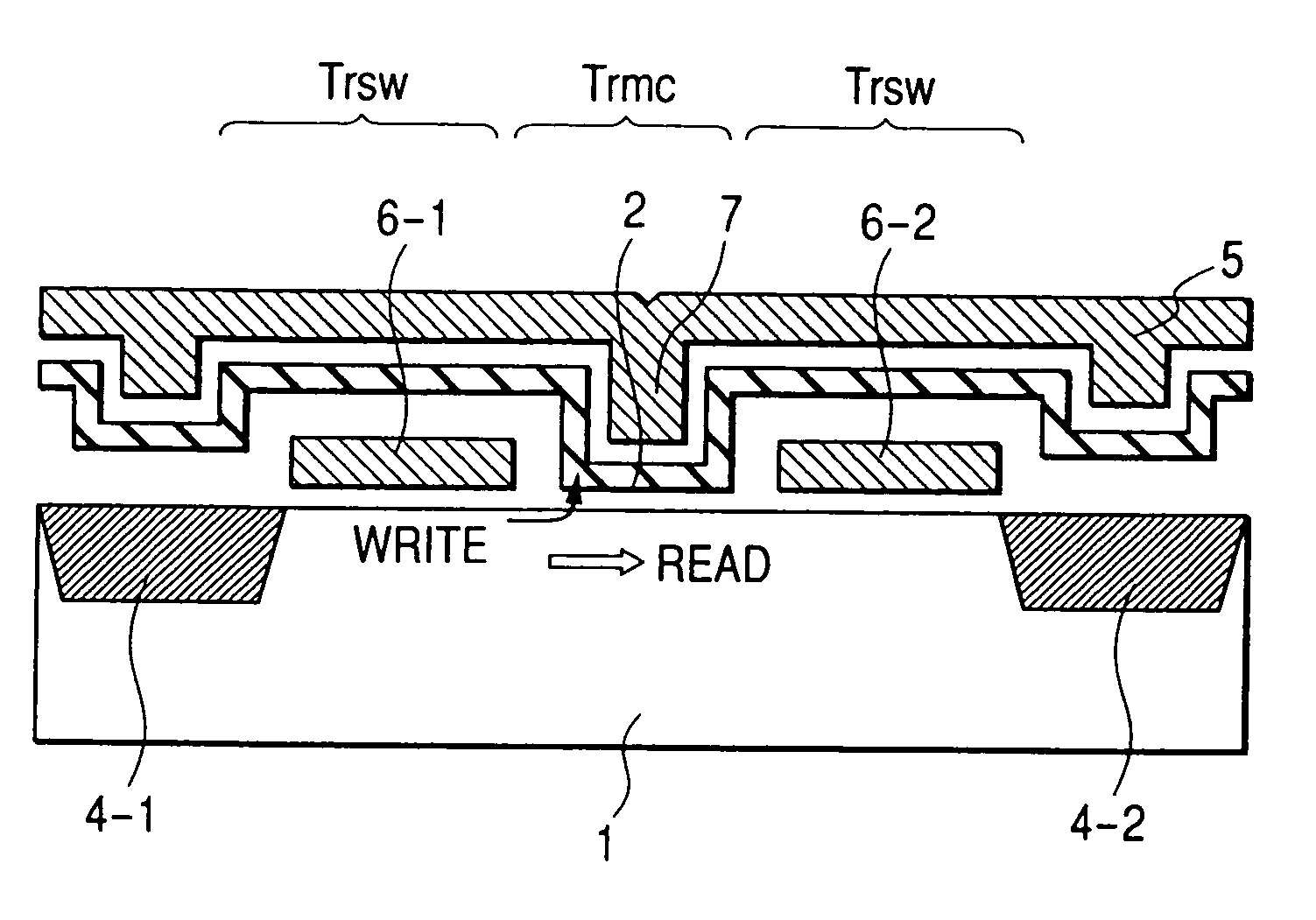
[0140] A memory cell structure, in which switch transistors Trsw are disposed on both the sides of a memory transistor Memory transistor Trmc, is employed as a first embodiment of a multi-storage nonvolatile memory cell in order to solve the problems of an increase in programming speed in program, read disturb during read, and an expansion of a dual-way signal read margin. While a certain amount of reduction of a degree of density cannot help being sacrificed by the provision of the switch transistors Trsw on both the sides of the memory transistor Trmc, FIGS. 14 to 16 exemplify a structure in which a reduction of the degree of density is suppressed utilizing self-aligning diffusion. It should be understood that the term “transistor” used in the specification is an expression conveniently used to make it easy to understand the structure of the multi-storage nonvolatile memory cell according to the present invention and does not mean a perfect transistor, and it is only...
second embodiment
OF MEMORY CELL
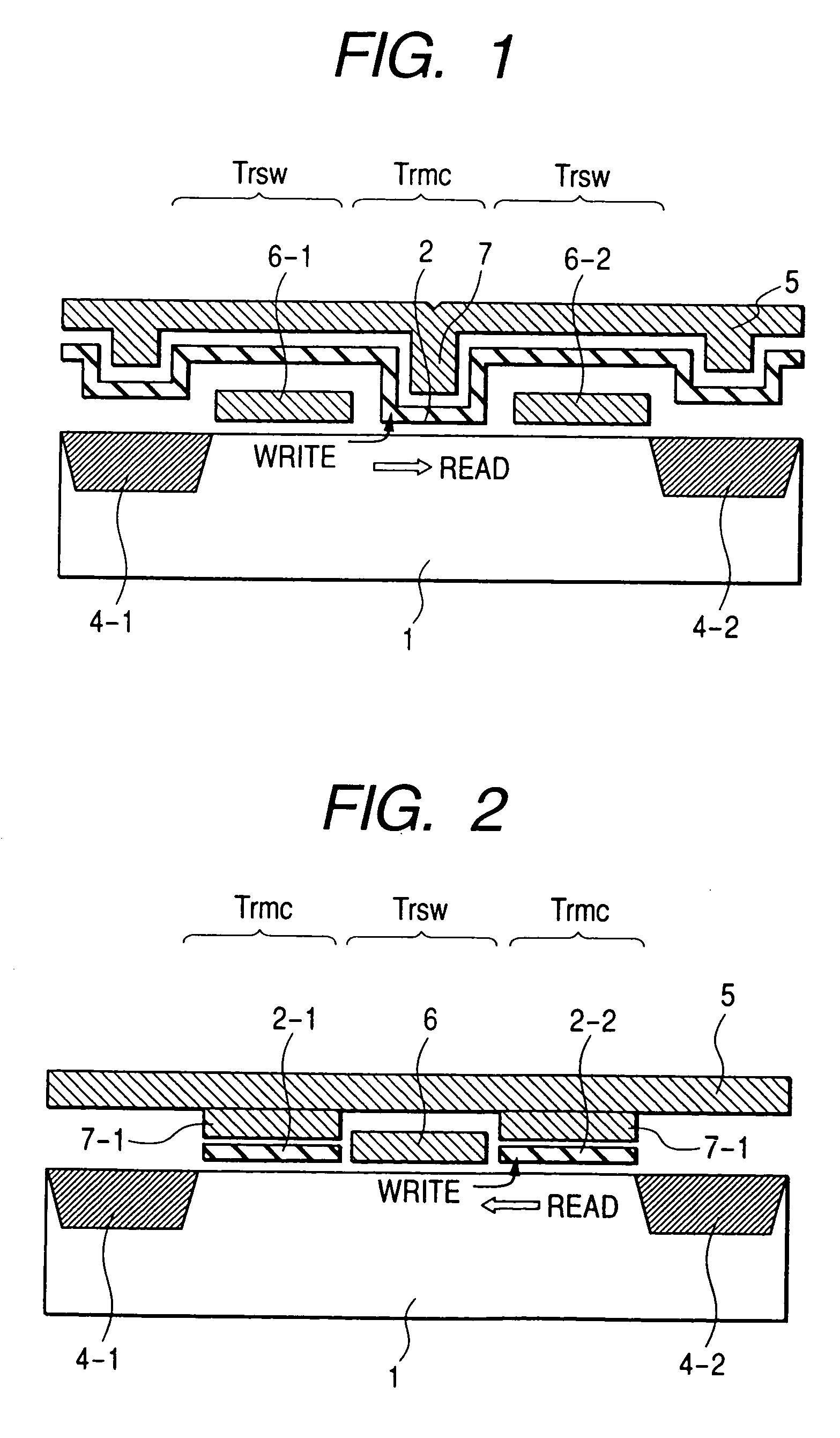
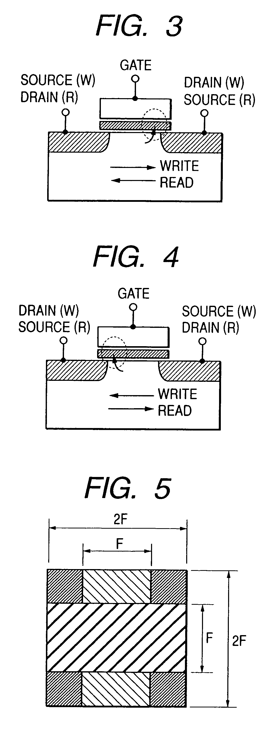
[0171] FIGS. 41 to 43 exemplify a second embodiment of a memory cell. The memory cell shown in the figures has such a structure that switch transistors Trsw are formed on both the sides of a memory transistor Trmc by diffusion using a self-aligned side-wall gate processing technology. In this case, a gate length of each switch transistor Trsw can be processed to about one half a technology feature size F. Accordingly, as apparent from FIG. 43, a size of the memory cell per one bit can be regarded as 3F2 while a size of the memory cell is 6F2, and thus a cell size, which is about one half a conventional cell size, is realized, whereby high density can be achieved. Since the transistors in the memory cell are disposed and lined entirely similarly to those of the memory cell provided according to FIGS. 14 to 16, it is possible to carry out program at high speed, to reduce deterioration of program, to avoid read disturb, and to expand a signal detection margin.
[0172]FIG. ...
third embodiment
OF MEMORY CELL
[0182]FIG. 52 exemplifies a cross section of a memory cell of a third embodiment and FIG. 53 exemplifies a layout thereof. The memory cell of the third embodiment is arranged such that the MOS inversion layers of switch transistors Trsw are used as lines in place of the lines of the diffusion layers 4-1 and 4-2 in the memory cell of the first embodiment. That is, one memory cell has a memory cell structure including one memory transistor Trmc, two switch transistors Trsw and two transistor inversion layer lines 20-1 and 20-2. The memory transistor Trmc includes a gate insulating film 2 having the discrete traps, the memory gate electrode 7 of the memory transistor Trmc is connected to word lines 5, the two transistor inversion layer lines 20-1 and 20-2 form source lines and bit lines as well as the two switch transistors Trsw and the two transistor inversion layer lines 20-1 and 20-2, which form the source lines and the bit lines, share gate electrodes 6-1 and 6-2, res...
PUM
 Abstract
Description
Claims
Application Information
 - R&D
- Intellectual Property
- Life Sciences
- Materials
- Tech Scout
- Unparalleled Data Quality
- Higher Quality Content
- 60% Fewer Hallucinations
Browse by: Latest US Patents, China's latest patents, Technical Efficacy Thesaurus, Application Domain, Technology Topic, Popular Technical Reports.
© 2025 PatSnap. All rights reserved.Legal|Privacy policy|Modern Slavery Act Transparency Statement|Sitemap|About US| Contact US: help@patsnap.com