High voltage mosfet having Si/SiGe heterojunction structure and method of manufacturing the same

a high-voltage metal oxide semiconductor and heterojunction technology, which is applied in the direction of basic electric elements, electrical apparatus, semiconductor devices, etc., can solve the problems of difficult to precisely control the on resistance of the channel region, and achieve low resistance, high breakdown voltage, and reduced transconductance (gm).

Active Publication Date: 2006-05-18
III HLDG 2
View PDF10 Cites 25 Cited by
  • Summary
  • Abstract
  • Description
  • Claims
  • Application Information

AI Technical Summary

Benefits of technology

[0013] The present invention is directed to a high voltage metal oxide semiconductor field effect transistor (HVMOSFET) and method of manufacturing the same, in which a channel has a Si / SiGe heterojunction structure so that a difficulty in ensuring a low on resistance due to a lightly doped n-type drift region and a reduction in transconductance (Gm) caused by a hot electron effect are overcome and also, a high breakdown voltage can be obtained.

Problems solved by technology

However, a low dopant concentration of the n-type drift region 14 makes it difficult to precisely control the on resistance of the channel region and precludes ensuring a low on resistance so as not to obtain a high driving current.

Method used


Image

  • High voltage mosfet having Si/SiGe heterojunction structure and method of manufacturing the same
  • High voltage mosfet having Si/SiGe heterojunction structure and method of manufacturing the same
  • High voltage mosfet having Si/SiGe heterojunction structure and method of manufacturing the same

Examples


Embodiment Construction

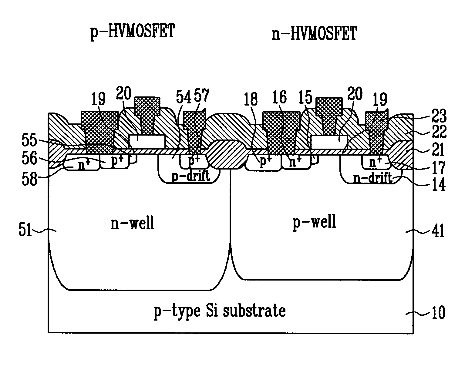
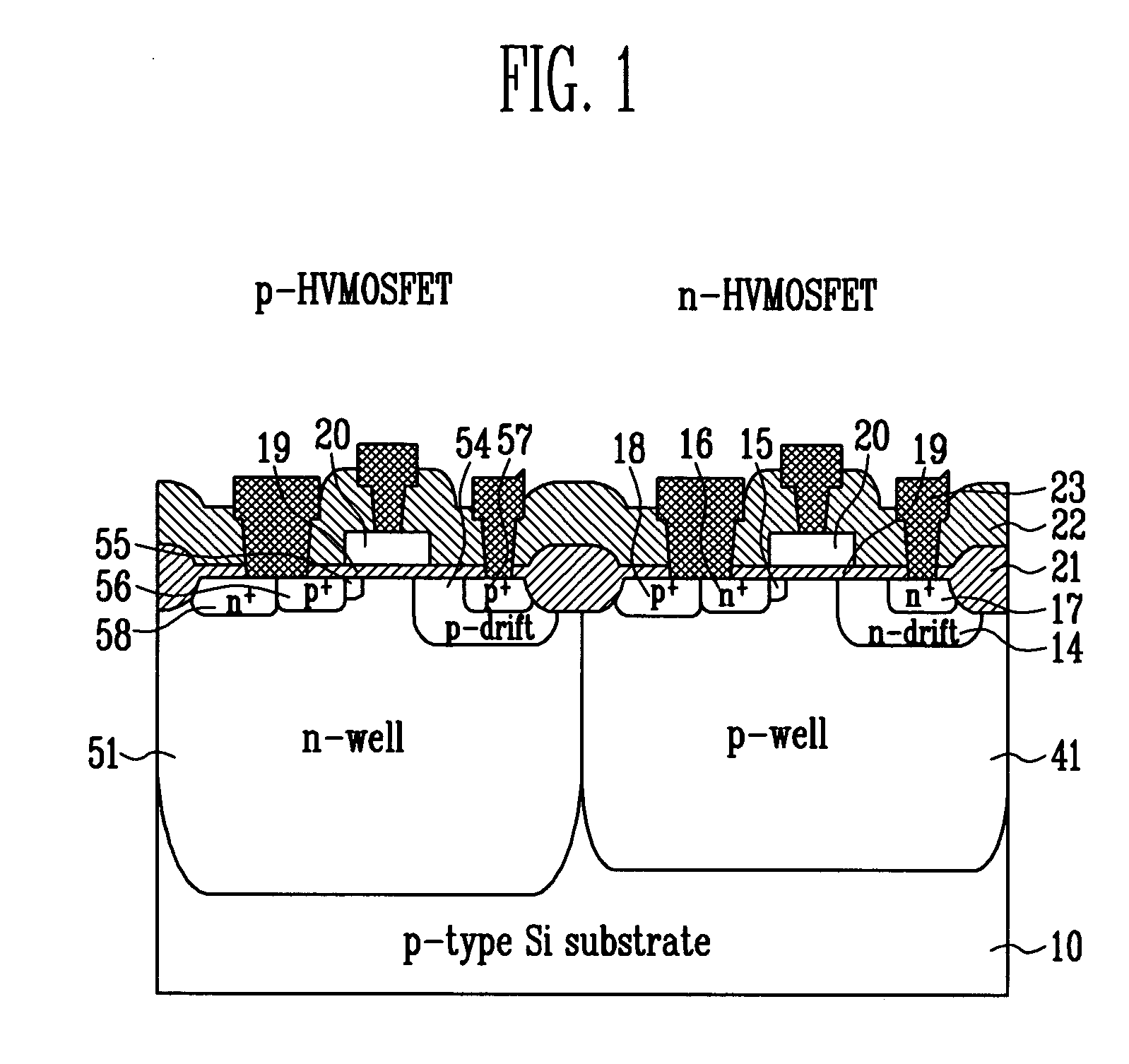
[0028] The present invention will now be described more fully hereinafter with reference to the accompanying drawings, in which exemplary embodiments of the invention are shown. This invention may, however, be embodied in different forms and should not be construed as limited to the embodiments set forth herein. Rather, these embodiments are provided so that this disclosure is thorough and complete and fully conveys the scope of the invention to those skilled in the art.

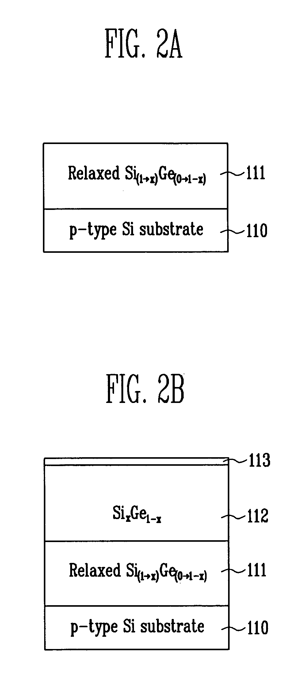
[0029]FIGS. 2A through 2F are cross-sectional views illustrating a method of manufacturing a high voltage metal oxide semiconductor field effect transistor (HVMOSFET) having a heterojunction structure according to an exemplary embodiment of the present invention.

[0030] Referring to FIG. 2A, a relaxed Si(1→x)Ge(0→1-x) epitaxial layer 111 is formed on a silicon substrate 110. The relaxed Si(1→x)Ge(0→1-x) epitaxial layer 111 is formed to a sufficient thickness of about 0.5 μm or more, a Ge content (x) is gradually inc...


PUM


Abstract

Provided are high voltage metal oxide semiconductor field effect transistor (HVMOSFET) having a Si/SiGe heterojunction structure and method of manufacturing the same. In this method, a substrate on which a Si layer, a relaxed SiGe epitaxial layer, a SiGe epitaxial layer, and a Si epitaxial layer are stacked or a substrate on which a Si layer having a well region, a SiGe epitaxial layer, and a Si epitaxial layer are stacked is formed. For the device having the heterojunction structure, the number of conduction carriers through a potential well and the mobility of the carriers increase to reduce an on resistance, thus increasing saturation current. Also, an intensity of vertical electric field decreases so that a breakdown voltage can be maintained at a very high level. Further, a reduction in vertical electric field due to the heterojunction structure leads to a gain in transconductance (Gm), with the results that a hot electron effect is inhibited and the reliability of the device is enhanced.

Description

CROSS-REFERENCE TO RELATED APPLICATION [0001] This application claims priority to and the benefit of Korean Patent Application No. 2004-94283, filed Nov. 17, 2004, the disclosure of which is incorporated herein by reference in its entirety. BACKGROUND [0002] 1. Field of the Invention [0003] The present invention relates to a power device and method of manufacturing the same and, more specifically, to a high voltage metal oxide semiconductor field effect transistor (HVMOSFET) having a Si / SiGe heterojunction structure and method of manufacturing the same, in which a breakdown voltage is held high and an on resistance is held low. [0004] 2. Discussion of Related Art [0005] In general, power devices using a field effect include a lightly doped drain-high voltage MOSFET (LDD-HVMOSFET), a double diffused MOSFET (DMOSFET), an extended drain MOSFET (EDMOSFET), and a lateral double diffused MOSFET (LDMOSFET). These power devices are being watched with keen interest as high voltage devices be...

Claims


Application Information

Patent Timeline
Patent Type & Authority Applications(United States)
IPC IPC(8): H01L21/8234
CPCH01L21/823807H01L29/1054H01L29/66659H01L29/7835H01L21/18
Inventor CHO, YOUNG KYUNKWON, SUNG KUROH, TAE MOONLEE, DAE WOOKIM, JONG DAE
Owner III HLDG 2
Why Eureka
Try Eureka