
Installation for processing a substrate

Inactive Publication Date: 2006-05-25
EVATEC +1
View PDF23 Cites 27 Cited by
  • Summary
  • Abstract
  • Description
  • Claims
  • Application Information

AI Technical Summary

Benefits of technology

[0012] It is an object of the invention to provide an installation which belongs to the technical field mentioned above, has a simple structure, is easy to maintain and in which a thin and / or large-area, mechanically sensitive substrate can be processed without the risk of damage or destruction.

Problems solved by technology

Otherwise, there is a risk of the wafer being excessively heated, which can lead to damage or destruction of the wafer.
The large surface area and low thickness of these substrates (typically 0.8 mm or less) impose additional mechanical demands both on the holding of the wafers while they are being processed and on the transporting of the wafers through the vacuum process installation, since even low levels of forces can lead to damage or destruction of the substrates.
At the same time, good dissipation of the process heat which occurs, for example, in sputtering processes has to be ensured, since otherwise the thin substrates, with their low heat capacity, will very quickly reach temperatures of more than 150° C., at which existing layer systems on the wafers can already be damaged.
Moreover, even when heated to temperatures lower than this, there is a risk of internal thermal stresses occurring in a layer which has been deposited on the substrate, and during cooling these stresses lead to deformation of this layer.
Dissipation of the process heat is difficult in vacuum chambers since the heat transfer has to be effected primarily through thermal radiation.
However, the mechanical transport and holding apparatuses disclosed in these documents are relatively unsuitable for large-area substrates with a low thickness, since the holding forces are unevenly distributed over the wafer, resulting in mechanical stresses.
This means that it is impossible to achieve effective cooling for thin substrates.
However, the chuck is complex to produce and requires frequent maintenance; in particular, the component which contact-connects the substrate has to be replaced at regular intervals.
This is generally done using spaced-apart pins, and if the chuck is insufficiently discharged can lead to damage or destruction of the substrate.

Method used


Image

  • Installation for processing a substrate
  • Installation for processing a substrate
  • Installation for processing a substrate

Examples


first embodiment

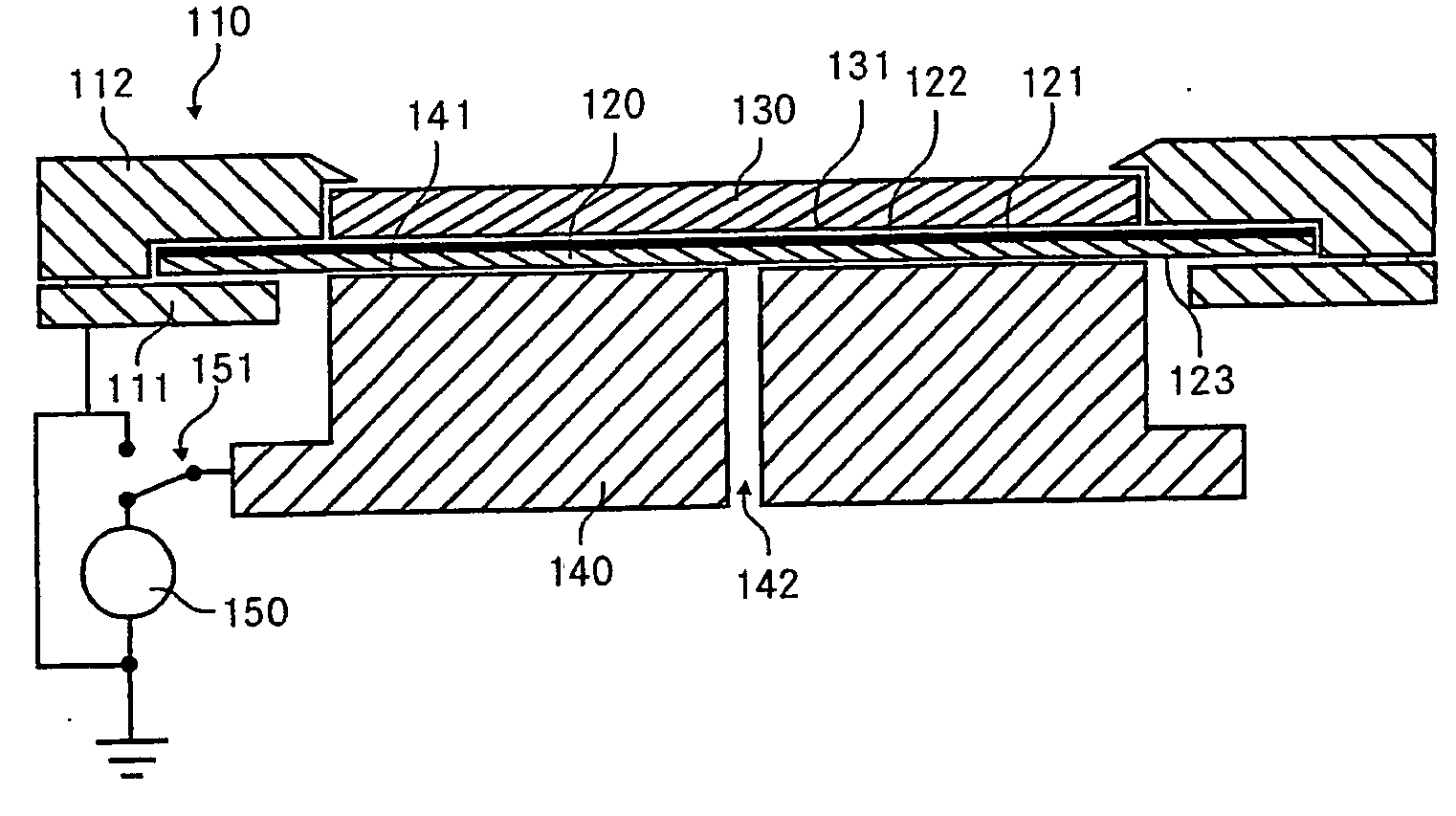
[0044]FIG. 1 diagrammatically depicts a unipolar electrode and a holding and transport frame of a processing station according to the invention. For the sake of clarity, the length ratios of the components illustrated do not correspond to those used in reality (the same also applies to the following figures). A carrier film 120, to which a large-area and thin substrate 130 has been secured, is clamped in a frame 110. The substrate 130 is, for example, a circular, thinned semiconductor wafer with a diameter of 300 mm and a thickness of 200 μm.

[0045] The dimensions of the frame 110 are such that the substrate 130 can be secured over its entire surface to the carrier film 120 clamped in the frame 110. The securing is effected between the underside 131 of the substrate 130 and the upper main surface 121 of the carrier film 120, by means of a vacuum-compatible, advantageously thermally conductive adhesive which is subsequently easy to release again. The frame 110 is composed of an annula...

fourth embodiment

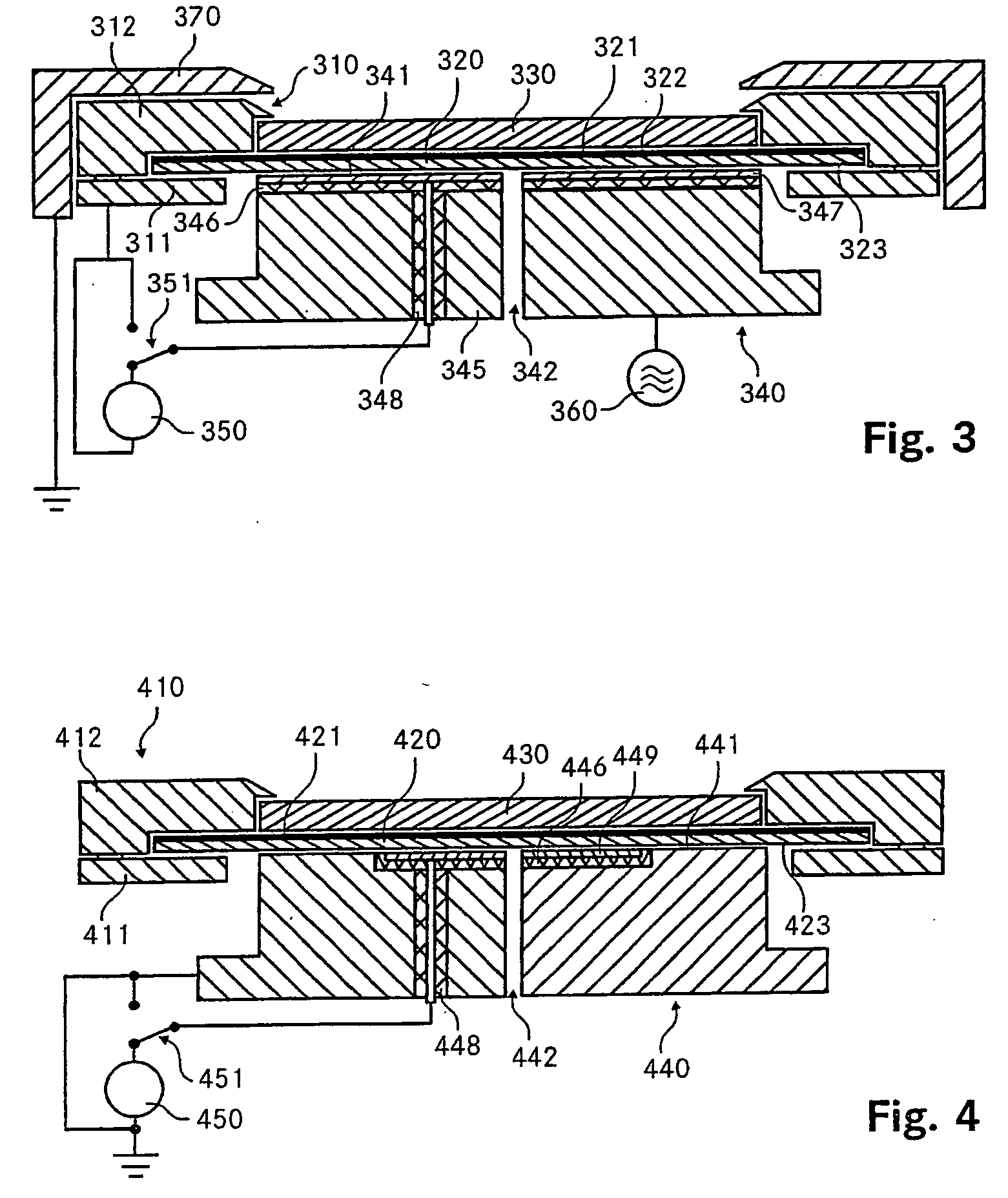
[0067]FIG. 4 diagrammatically depicts a bipolar electrode and a holding and transport frame of a processing station according to the invention.

[0068] The mechanical structure and arrangement of the frame 410 are identical to the frame of the first and third embodiments, as illustrated in FIGS. 1 and 3. Once again, the carrier film 420 of polyimide with a thickness of 100 μm, to which the substrate 430 is secured over a large area, is clamped in the frame 410. The frame 410 is composed of an annular bottom part 411 and a corresponding annular top part 412 releasably connected to the bottom part, with the carrier film 420 clamped between the two parts of the frame.

[0069] The frame 410 with the clamped-in carrier film 420 is arranged adjacent to a planar upper outer surface 441 of a metallic electrode 440, with the lower main surface 423 of the carrier film 420 positioned parallel to and at a short distance from the upper outer surface 441 of the electrode 440. The surface area and sh...


PUM

PropertyMeasurementUnit
Lengthaaaaaaaaaa
Lengthaaaaaaaaaa
Lengthaaaaaaaaaa

Abstract

The invention relates to an installation, in particular a vacuum processing installation for processing a substrate (130), in particular a semiconductor wafer, comprising a processing station. Said installation comprises a frame (110), to which is clamped a carrier (120), for holding and / or transporting the substrate (130), whereby the latter (130) can be fastened by its entire surface to said carrier (120). The processing station preferably comprises a chuck electrode (140) with a flat outer surface (141) and the carrier (120) can be positioned parallel and adjacent to said outer surface (141) of the chuck electrode (140). The carrier is composed in particular of a non-conductive dielectric material and is provided on one side with a conductive layer (122), in such a way that the chuck electrode (140) and the carrier (120) form an electrostatic chuck.

Description

FIELD OF THE INVENTION [0001] The invention relates to an installation, in particular a vacuum process installation, for processing a substrate, in particular a semiconductor wafer, having at least one processing station. The invention also relates to a processing station for an installation of this type, to a frame for an installation of this type, for holding and / or transporting the substrate, to a film which is to be clamped into the frame and to a method for processing a substrate, in particular a semiconductor wafer, in a vacuum process installation. PRIOR ART [0002] Semiconductor wafers for the production of integrated circuits are usually processed in vacuum process installations which comprise one or more processing stations, in which the wafer is etched or coated in a vacuum chamber, e.g. by means of a CVD (chemical vapor deposition) or PVD (physical vapor deposition) process. In this context, it is important for the wafer to be held in a mechanically stable position in the...

Claims


Application Information

Patent Timeline
IPC IPC(8): C25D5/56H01L21/00H01L21/68
CPCC25D17/06C25D17/12Y10T279/23C25D17/001C25D7/123C23C14/50H01L21/6833H01L21/68721C23C16/4585C23C16/4586H01L21/68C23C16/4583
Inventor WEICHART, JURGEN
Owner EVATEC
Learn More