Methods and apparatus for forming a titanium nitride layer

Inactive Publication Date: 2006-05-25
SAMSUNG ELECTRONICS CO LTD
View PDF11 Cites 28 Cited by
  • Summary
  • Abstract
  • Description
  • Claims
  • Application Information

AI Technical Summary

Benefits of technology

[0014] Example embodiments of the present invention provide a method of rapidly forming a titanium nitride layer as part of a semiconductor element such that the titanium nitride

Problems solved by technology

Hafnium (IV) chloride may adversely affect the dielectric characteristics of the dielectric layer.
Further, chlorine ions remaining in the titanium nitride layer may also damage the semiconductor device by increasing a specific resistance of the titanium nitride layer, thereby augmenting a con

Method used


Image

  • Methods and apparatus for forming a titanium nitride layer
  • Methods and apparatus for forming a titanium nitride layer
  • Methods and apparatus for forming a titanium nitride layer

Examples


Example

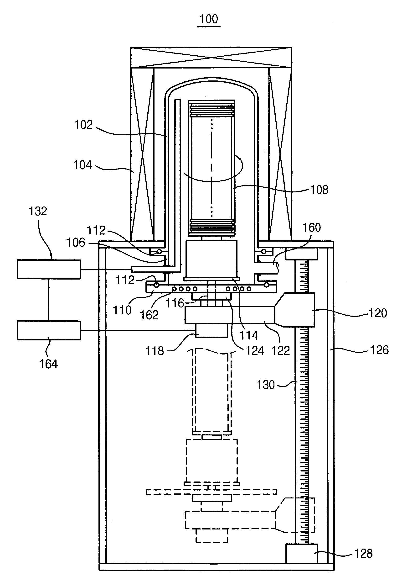
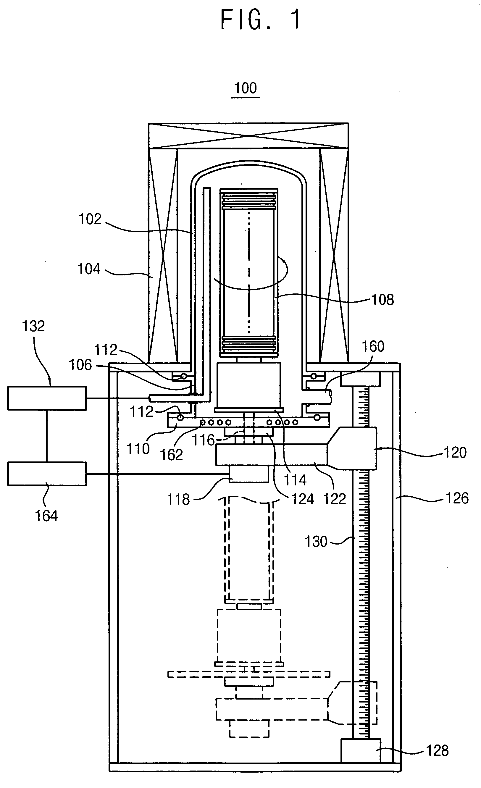
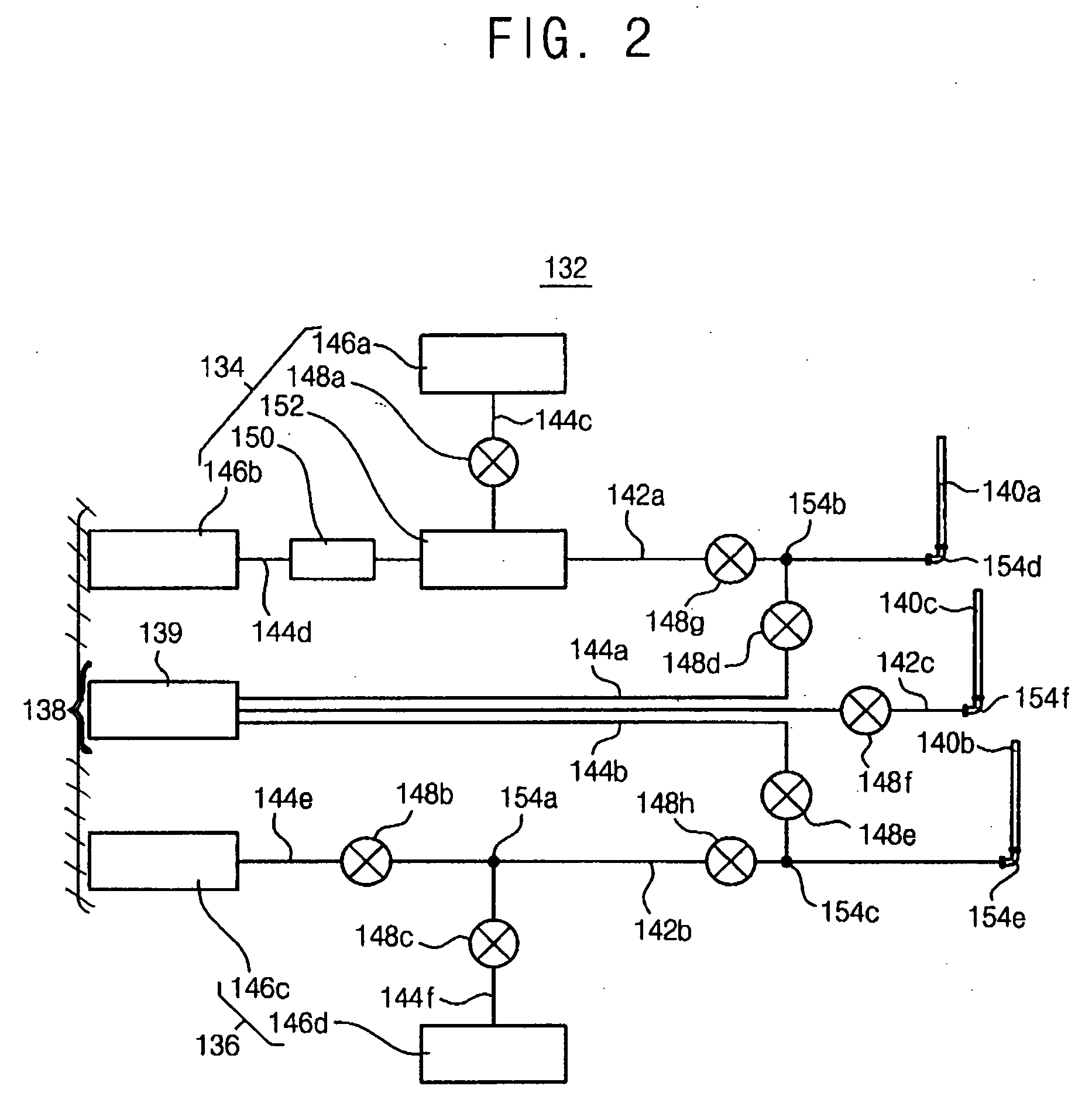
[0051] The present invention is described more fully hereinafter with reference to the accompanying drawings, in which illustrative embodiments of the present invention are shown. The present invention may, however, be embodied in many different forms and should not be construed as limited to the embodiments set forth herein. Rather, these embodiments are provided so that this disclosure will be thorough and complete, and will fully convey the scope of the invention to those skilled in the art. In the drawings, the sizes and relative sizes of layers and regions are sometimes exaggerated for clarity.

[0052] It will be understood that when an element or layer is referred to as being “on”, “connected to” or “coupled to” another element or layer, it can be directly on, connected or coupled to the other element or layer, or intervening elements or layers may be present. In contrast, when an element is referred to as being “directly on,”“directly connected to” or “directly coupled to” ano...


PUM

PropertyMeasurementUnit
Temperatureaaaaaaaaaa
Timeaaaaaaaaaa

Abstract

A method of forming a titanium nitride layer by an atomic layer deposition process using a batch-type vertical reaction furnace is described wherein a first source gas including a titanium precursor is provided onto substrates loaded in a process chamber for a first time period; a first purge gas is introduced into the process chamber for a second time period shorter than the first time period; a second source gas including nitrogen is provided onto the substrates for a third time period substantially identical to the first time period; and, a second purge gas is introduced into the process chamber for a fourth time period substantially identical to the second time period. Titanium nitride layers having uniform thickness and good step coverage may thus be formed while realizing a greatly reduced manufacturing time.

Description

CROSS-REFERENCE TO RELATED APPLICATION [0001] This application claims the benefit of priority under 35 USC § 119 to Korean Patent Application No. 2004-94980, filed on Nov. 19, 2004, the disclosure of which is incorporated herein by reference in its entirety. BACKGROUND OF THE INVENTION [0002] 1. Field of the Invention [0003] Example embodiments of the present invention relate to methods used in forming a layer on a substrate and to an associated apparatus for forming the layer on the substrate. More particularly, example embodiments of the present invention relate to methods of forming a titanium nitride (TiN) layer on a semiconductor substrate and to an apparatus for forming the titanium nitride layer on the semiconductor substrate. [0004] 2. Description of the Related Art [0005] Semiconductor devices are typically manufactured by executing various sequential processes on suitable semiconductor substrates such as on silicon wafers. For example, a deposition process is generally per...

Claims


Application Information

Patent Timeline
IPC IPC(8): C23C16/00B05C11/00
CPCC23C16/34C23C16/45546H01L21/28556H01L21/67109H01L21/67757H01L21/20
Inventor HWANG, WAN-GOOKIM, MYEONG-JINCHAE, SEUNG-KILIM, HYUN-SEOKJANG, KYOUNG-HO
Owner SAMSUNG ELECTRONICS CO LTD
Why Eureka
Try Eureka