Direct liquid injection system and method for forming multi-component dielectric films

a dielectric film and liquid injection system technology, applied in the direction of chemically reactive gases, coatings, crystal growth processes, etc., can solve the problems of increasing power dissipation, current leakage, chemical and thermal instability of materials on silicon,

Inactive Publication Date: 2006-05-25
AVIZA TECHNOLOGY INC
View PDF3 Cites 197 Cited by
  • Summary
  • Abstract
  • Description
  • Claims
  • Application Information

AI Technical Summary

Benefits of technology

[0010] One aspect of the present invention provides systems and methods for fabricating multi-component dielectric films by mixing vaporized precursors together and then injecting or co-injecting the vaporized precursors such that a mixture of precursors are present in the ALD chamber. As used herein the term “multi-component” film means that the film contains two or more metal or metalloid elements. A variety of multi-component films may be formed by the present invention, including but not limited to: metal, metal alloy, mixed metal oxides, silicates, nitrides, oxynitrides, and mixtures thereof.
[0011] In one embodiment of the present invention, a method of forming a thin film on a surface of a substrate by atomic layer deposition is provided, characterized in that: two or more vaporized precursors, each of the precursors containing at least one different chemical component (typically a metal or metalloid element), are conveyed into a process chamber together to form a monolayer on the surface of the substrate, and said monolayer contains each of the separate chemical components. In general the term co-injecting is used to mean that two or more precursors having at least one different chemical component are present in a chamber such that a film is produced having multiple components. This may be accomplished by injecting or conveying precursors together in either vapor or liquid state (aerosol) into a process chamber, or mixing the precursors in the process chamber. Mixing of the precursors prior to introduction into the process chamber is preferred, but not required.
[0012] In another aspect the present invention provides a system for forming multi-component films. In one embodiment, the system generally includes one or more vaporizers, each vaporizer being coupled to a manifold. The manifold is configured to mix the vaporized precursors generated by the vaporizers. The manifold is coupled to an inlet to a process chamber and the mixed precursors are injected into the chamber through the inlet. In one embodiment the inlet is comprised of an injector, such as a showerhead injector. It is possible that the precursors may be mixed in the injector, and not in a manifold.
[0013] In yet another aspect of the present invention, systems and methods are provided wherein the process chamber is configured in such a manner as to practice said deposition method on a single substrate. Alternatively, systems and methods are provided wherein the process chamber is configured in such a manner as to practice said deposition methods on a plurality of substrates, typically numbering between 1 and 200 substrates. As an example, it would be possible to process between 1 and 200 substrates when the substrates are silicon wafers with a diameter of 200 mm. More typically, it would be possible to process between 1 and 150 substrates when the substrates are silicon wafers with a diameter of 200 mm. If the substrates are silicon wafer with a diameter of 300 mm, it would be more typical to process between 1 and 100 substrates. Recently, a new version of “mini-batch” reactor has been established in the market whereby a batch of substrates numbering between 1 and 50 would be processed in a single batch. In this case, the substrates would be silicon wafers with diameters of either 200 mm or 300 mm. Finally, some of the new “mini-batch” systems are configured to process between 1 and 25 substrates. Again, in this case, the substrates would be silicon wafers with diameters of either 200 mm or 300 mm.
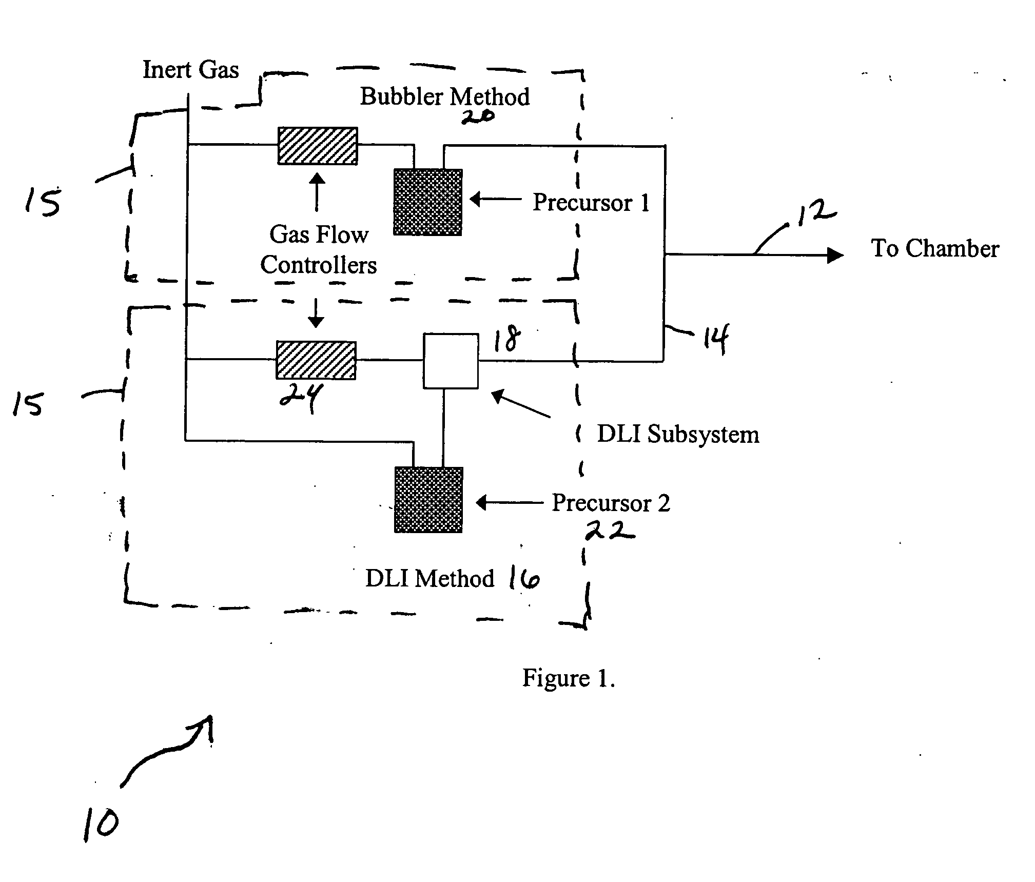
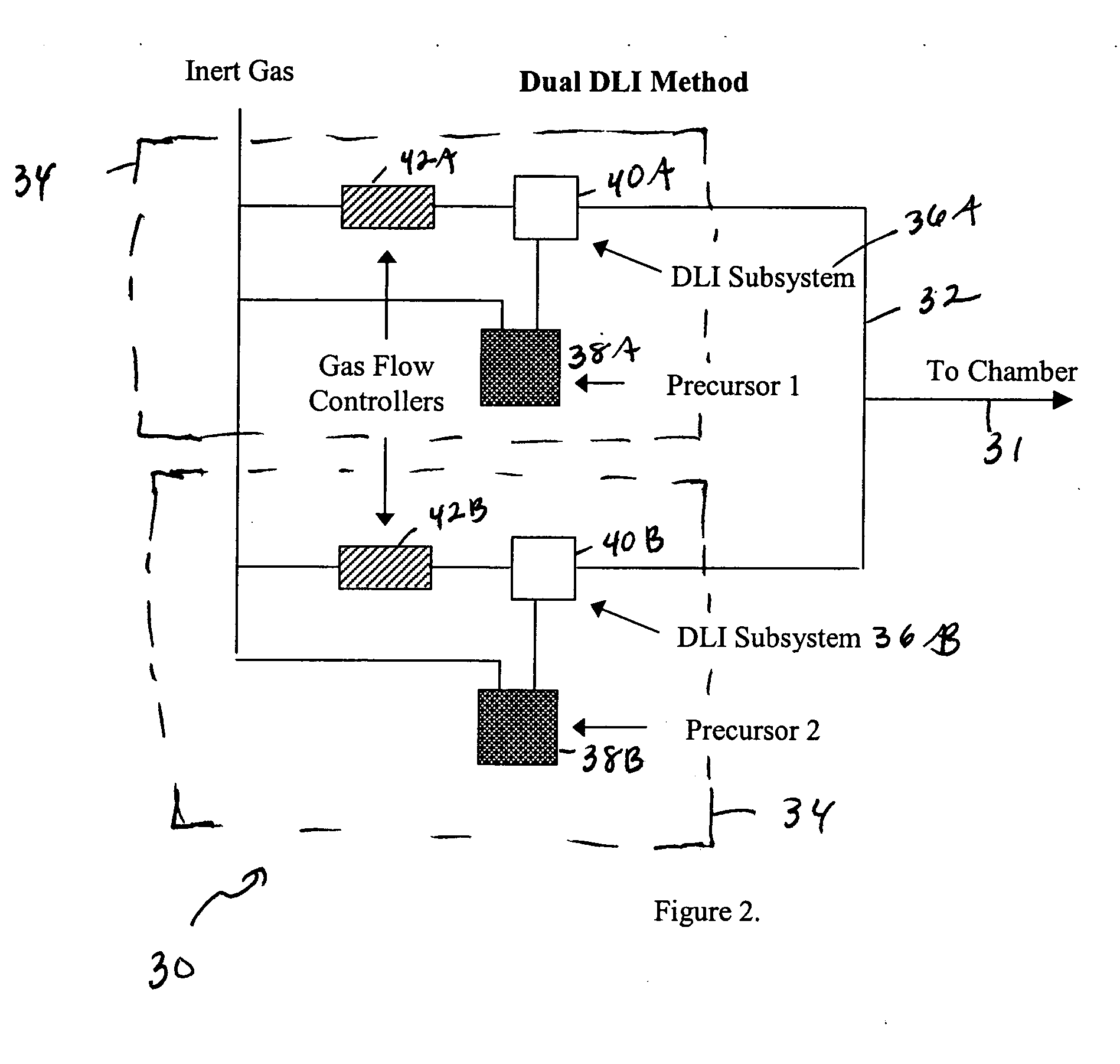
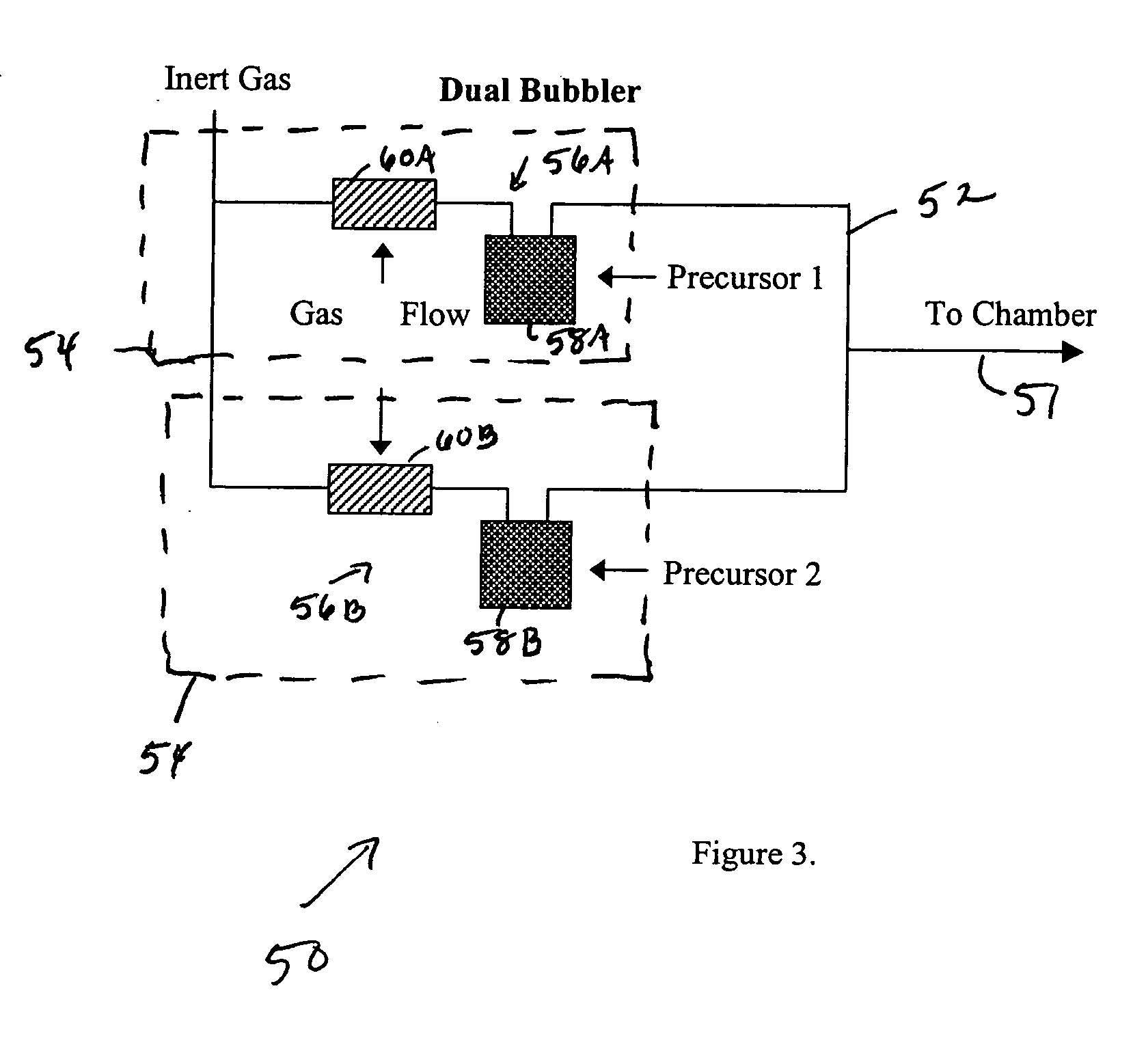
[0014] In a further embodiment, a method of forming a film of a surface of a substrate is provided, characterized in that: two or more precursors, each of the precursors comprising at least one different chemical component are provided, a desired amount of said precursors are converted to a gaseous state by at least one or both of a direct liquid injection system and a bubbler system, said precursors in the gaseous state are conveyed to a process chamber together and form a monolayer on the surface of the substrate, said monolayer containing each of the separate chemical components.
[0015] In another aspect, a system for atomic layer deposition (ALD) is provided comprising: at least one direct liquid injection system configured to inject one or more deposition precursors into one or more vaporization chambers, at least one bubble system configured to vaporize one or more deposition precursors; and a process chamber coupled to said direct liquid injection system and said bubblers system, said process chamber being configured to receive the deposition precursors from said direct liquid injection and bubbler systems and being adapted to carry out an ALD process.

Problems solved by technology

However, as traditional silicon-based transistor geometries reach a critical point where the silicon dioxide gate dielectric becomes just a few atomic layers thick, tunneling of electrons will become more prevalent leading to current leakage and increase in power dissipation.
Unfortunately, these materials are chemically and thermally unstable on silicon, unlike silicon dioxide, forming defects and charge traps at the interface between the metal dielectric and the silicon substrate.
The charge traps and defects interact with the voltage applied at the gate and perturb the performance and reliability of the transistor.
The silicon dioxide interface buffers the silicon substrate from the dielectric, but the silicon dioxide interface may not be compatible with the surface properties of the dielectric.
Prior art deposition techniques for fabricating films such as chemical vapor deposition (CVD) are increasingly unable to meet the requirements of advanced thin films.
While CVD processes can be tailored to provide conformal films with improved step coverage, CVD processes often require high processing temperatures.
For instance, one of the obstacles of making high-k gate dielectrics is the formation of an interfacial silicon oxide layer during CVD processes.
Another obstacle is the limitation of prior art CVD processes in depositing ultra thin films for high k gate dielectrics on a silicon substrate.
This approach of building up layers of different laminate films leads to many electron traps in the film due to the multiple interfaces which requires a high temperature thermal anneal to fix the traps.
The addition of the high temperature thermal annealing step increases cost and time for manufacturing semiconductors, and moreover can result in the undesirable out migration of elements from previously formed layers on the wafer.
In addition, it is difficult to control the stoichiometric composition of multi-component films in the laminate method.
The dielectric constant (k), crystallization temperature and refractive index of HfSiOx, films cannot be easily controlled by the traditional one chemical sequential precursor pulse methods (such as the laminate method).
Furthermore, the cycle times needed to form a film of desired thickness using the conventional sequential pulse and purge of one chemical precursor at a time are impractical and require too much time for future IC manufacturing.
Attempts to fabricate multi-component films using mixed precursors have been limited to the traditional CVD methods.
There are several drawbacks associated with the method described in the '613 and '734 patents.
One of the major drawbacks of the prior art is the limitation in film composition control.
In addition, even if appropriate volumes of samples are provided, there is no guarantee that the mixture will vaporize uniformly since each precursor has a unique boiling point, vapor pressure and volatility.
Furthermore, if the discrepancy in boiling points between the precursors is substantial, one precursor may decompose at the boiling point of the second forming particulates or contaminants.
Generally, either the precursors have not been adequately mixed, resulting in a non-uniform film composition, or mixing of the two vapors causes pre-reaction in the gas phase, resulting in the formation of particles or contaminants that are deposited on the wafer.

Method used


Image

  • Direct liquid injection system and method for forming multi-component dielectric films
  • Direct liquid injection system and method for forming multi-component dielectric films
  • Direct liquid injection system and method for forming multi-component dielectric films

Examples


Embodiment Construction

[0023] In general, the inventor has discovered a method that provides for mixing precursors such that a mixture of precursors are present in a chamber during a single pulse step in an atomic layer deposition (ALD) process to form a monolayer having multiple chemical compounds on the surface of a substrate. The precursors are comprised of different chemical components, and such components will form the multi-component film. Such a method is a departure from the prior art, where the vaporized precursors are conveyed or pulsed separately into the chamber in the ALD process. A variety of multi-component films may be formed by the present invention, including but not limited to: metal, metal alloy, mixed metal oxides, silicates, nitrides, oxynitrides, and mixtures thereof.

[0024] In one aspect, the present invention provides a system and method for reproducibly and substantially uniformly controlling the stoichiometric composition of a multi-component film.

[0025] In a series of embodime...


PUM

PropertyMeasurementUnit
pressureaaaaaaaaaa
diameteraaaaaaaaaa
diameteraaaaaaaaaa

Abstract

The present invention provides methods and systems for atomic layer deposition (ALD). In some embodiments a system is provided comprising: at least one direct liquid injection system configured to inject one or more deposition precursors into one or more vaporization chambers, at least one bubble system configured to vaporize one or more deposition precursors; and a process chamber coupled to said direct liquid injection system and said bubblers system, said process chamber being configured to receive the deposition precursors from said direct liquid injection and bubbler systems and being adapted to carry out an ALD process. In an alternative embodiment, the system is comprised of two separate bubbler systems. In another alternative embodiment, the system is comprised of two separate direct liquid injection systems.

Description

CROSS REFERENCE TO RELATED APPLICATIONS [0001] This application claims the benefit of, and priority to, U.S. Provisional Patent application Ser. No. 60 / 602,189 filed Aug. 16, 2004, the disclosure of which is incorporated by reference herein in its entirety.FIELD OF THE INVENTION [0002] In general, the present invention relates to systems and methods for forming thin films in semiconductor applications. More specifically, the present invention relates to systems and methods for fabricating multi-component thin films on a substrate using mixed vaporized precursors. BACKGROUND OF THE INVENTION [0003] Concurrent with the increase in sophistication and drive towards miniaturization of microelectronics, the number of transistors per integrated circuit has exponentially grown and promises to grow to meet the demands for faster, smaller and more powerful electronic systems. However, as traditional silicon-based transistor geometries reach a critical point where the silicon dioxide gate diel...

Claims


Application Information

Patent Timeline
Patent Type & Authority Applications(United States)
IPC IPC(8): H01L21/31
CPCC23C16/34C23C16/4481C23C16/45512C23C16/45523C23C16/45544C23C16/45546C30B25/02C30B25/14H01L21/28562H01L21/3141H01L21/3144H01L21/31645H01L21/3185H01L21/02205H01L21/0228H01L21/02142H01L21/02175H01L21/20
Inventor SENZAKI, YOSHIHIDE
Owner AVIZA TECHNOLOGY INC
Why Eureka
Try Eureka