Wafer bonded silicon radiation detectors

a radiation detector and silicon technology, applied in the field of radiation detectors, can solve the problems of time-consuming and expensive to drift thick si(li) detectors, difficult to operate intrinsic detectors, and high cost of manufacturing double-sided detectors

Inactive Publication Date: 2006-06-08
PHLIPS BERNARD +3
View PDF8 Cites 14 Cited by
  • Summary
  • Abstract
  • Description
  • Claims
  • Application Information

AI Technical Summary

Problems solved by technology

However, manufacturing double-sided detectors is more expensive than conventional wafer processing techniques that are designed for single-sided wafer processing.
However, it is difficult to operate intrinsic detectors (with typical resistivities of 20,000 ohm-cm) with thicknesses greater than 2-3 mm due to well-known problems associated with high voltage break down.
These problems are a result of the voltage required to achieve full depletion, which varies as the square of the thickness.
However, this method has significant drawbacks in that it is time consuming and expensive to drift thick Si(Li) detectors, taking several months to drift a detector that is 1 cm thick.
Furthermore, these Si(Li) detectors typically have to be operated cold (approximately −50° C.) and are very susceptible to higher leakage currents following vacuum and temperature changes.
Additionally the detectors do not use standard CMOS or non-CMOS technology.
Accordingly, a crystal that is converted to higher resistivity to achieve the desired level of thickness still has significant drawbacks.
In addition to the issue of thickness, a disadvantage of germanium detectors is the liquid nitrogen temperature requirement for operation.

Method used


Image

  • Wafer bonded silicon radiation detectors
  • Wafer bonded silicon radiation detectors
  • Wafer bonded silicon radiation detectors

Examples


first embodiment

[0041] The direct wafer bonded silicon radiation detector as described above can be employed in a plurality of embodiments as will now be described. A first embodiment is illustrated in FIG. 5 illustrating a pixellated CMOS or non-CMOS detector 55. The detector is comprised of a pixellated top portion 60a disposed on wafer 60, which is direct wafer bonded to wafer 70 which is a thick, high resistivity semiconductor wafer.

[0042] In operation, a radiation source 56 emits a particle, gamma ray or x-ray, or other ionizing particles for example, at the under portion 70a of detector 55. The interaction of the emitted radiation and the voltage causes electron-hole pairs to be formed within detector 55. A voltage is applied to the detector 55, via voltage source 45. The electrons are then drifted to a first side 60b of wafer 60 through the pixellated surface 60a of wafer 60. By contrast, the holes are drifted to a second side 70b of wafer 70. The drifting of the electrons and holes can be r...

second embodiment

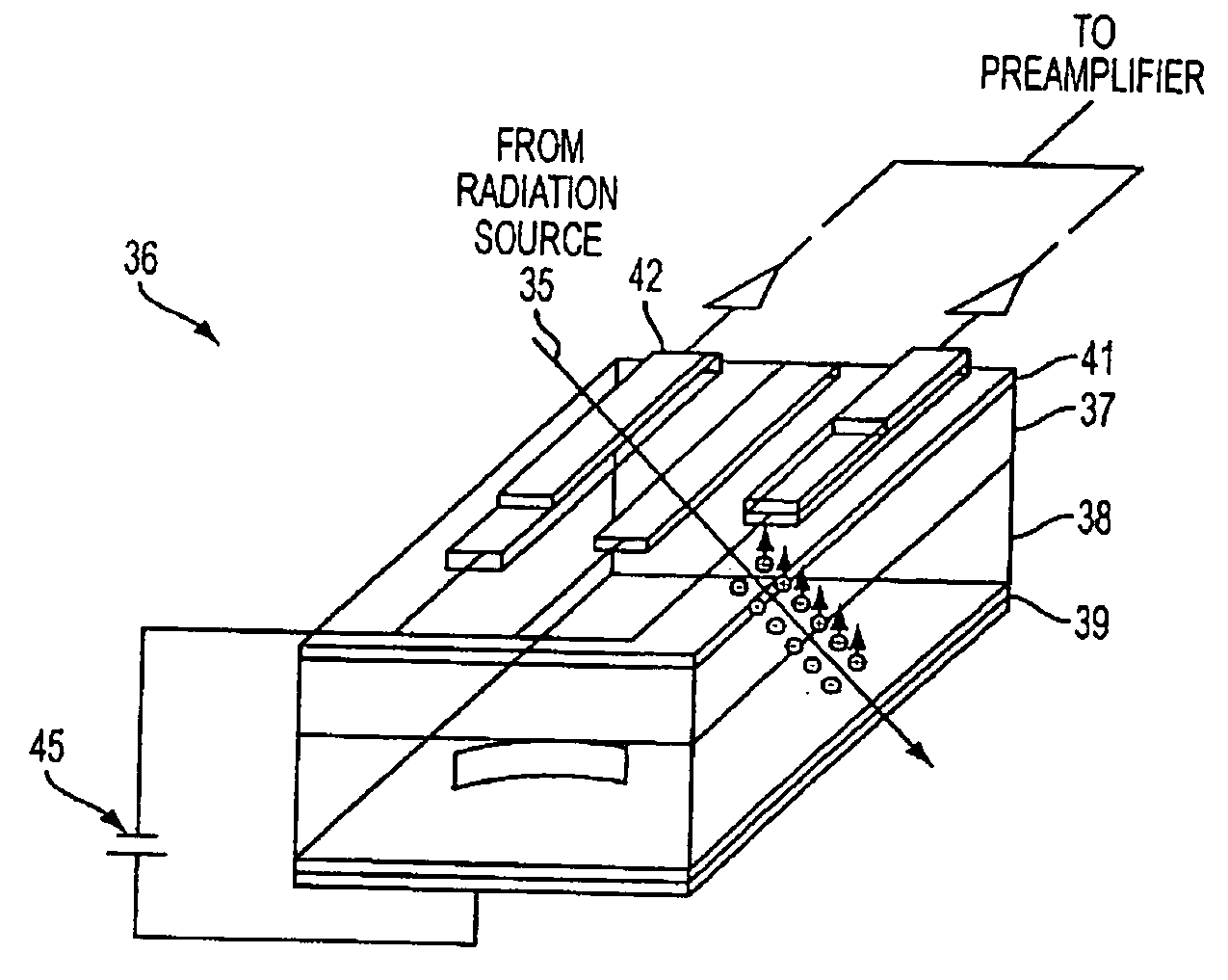
[0043] A second embodiment is depicted FIG. 6. This embodiment includes a double-sided strip surface on detector 75. The detector includes two relatively thin CMOS or non-CMOS device wafers 78 and 80 bonded together via the direct wafer bonding method mentioned above. The upper surface of wafer 78 comprises a plurality of conventional strip detectors 78a and is coupled to voltage source 45, and the lower portion of wafer 80 also comprises a plurality of strip detectors 80a. The strips 78a and 80a are positioned in an orthogonal pattern. Detector 75 preferably provides position-sensitive measurements employing strip detectors 78a and 80a for hard X-rays or penetrating particles, but with fewer readout channels required compared to the detector in FIG. 4.

[0044] The operation of detector 75 is similar to that of the detector 55 of FIG. 5. However, detector 75 employs strip detectors 78a and 80a, in a conventional fashion, in order to determine position information of the total drifted ...

third embodiment

[0045] A third embodiment depicted in FIG. 7. This device is a double-sided strip detector 85 made from two relatively thin CMOS or non-CMOS wafers 87, 89 direct wafer bonded on to a first side 92a and a second side 92b of a thick, high resisitivity semiconductor wafer 92. Conventionally, electrons would not be expected to diffuse through an interface of a thick high resistivity semiconductor wafer that has been bonded to another wafer. However, due to the unique properties of the wafer bonding process, electrons are able to diffuse through interfaces bonded through this process.

[0046] In operation, a gamma ray (not shown) is directed toward detector 85, a voltage, via voltage source 45 is applied to one of the thin CMOS or non-CMOS wafers 87 and 89. Electrons are drifted towards the direction of a surface of one of the wafers 87 and 89, whereas holes are drifted to the opposite directions of the electrons. The strip detectors on the surface of wafers 87 and 89 are then able to dete...


PUM


Abstract

An apparatus and method for operating a direct wafer bonded semiconductor radiation detector includes bonding a plurality of wafers, receiving a radiation signal from a radiation source thereby producing electron and hole pairs via the radiation signal interacting with the detecting device. A voltage source produces a voltage across the direct bonded wafers, thereby drifting the electrons and holes through the plurality of bonded layers. The drifted electrons and / or holes include total drifted charge information of the detector and are collected and processed either at the detector or remote from the detector.

Description

CROSS-REFERENCE TO RELATED APPLICATIONS [0001] This application claims benefit under 35 U.S.C. § 119(e) of a provisional U.S. patent application of Phlips et al entitled “Wafer Bonded Silicon Radiation Detectors”, Ser. No. 60 / 635,192, filed Dec. 3, 2004, the entire contents of the provisional application being incorporated herein by reference.BACKGROUND OF THE INVENTION [0002] 1. Field of the Invention [0003] The present invention relates generally to radiation detectors. More specifically the present invention relates to thick, high resistivity semiconductor radiation detectors formed through low temperature direct wafer bonding. [0004] 2. Description of Related Art [0005] Semiconductor detectors are based on crystalline semiconductor materials, most notably silicon and germanium. High-resolution x-ray and gamma ray detection preferably employ germanium and silicon detectors as the preferred detector technology. Germanium detectors in particular have been preferred due to their out...

Claims


Application Information

Patent Timeline
Patent Type & Authority Applications(United States)
IPC IPC(8): G01T1/24
CPCG01T1/24H01L27/14658
Inventor PHLIPS, BERNARDKUB, FRANCIS J.HOBART, KARL D.KURFESS, JAMES D.
Owner PHLIPS BERNARD
Why Eureka
Try Eureka