Press pack power semiconductor module

a technology of press pack and semiconductor module, which is applied in the direction of resistors, basic electric elements, solid-state devices, etc., can solve the problems of thermo-mechanical fatigue (also known as intermittent operating load, iol), fretting, and redundancy semiconductor devices introduced in the stack taking the additional load, so as to improve iol capability, reduce power dissipation, and improve thermal conductivity

Active Publication Date: 2006-06-08
HITACHI ENERGY SWITZERLAND AG
View PDF9 Cites 14 Cited by
  • Summary
  • Abstract
  • Description
  • Claims
  • Application Information

AI Technical Summary

Benefits of technology

[0011] The inventive module has an enhanced IOL capability due to CTE compatibility with the semiconductor and reduced power dissipation during normal operation when MMCs with higher thermal conductivities are used. It also has improved SCFM performance due to reduced power dissipation in the hotspot. Even if bowing in the plates occurs either during manufacture or during assembly processes (involving heating to facilitate bonding processes for eg soldering), the bow is flattened out by the use of a matrix comprising of Al or Ag and their alloys, under the pressure that the stack is subjected to in service giving a good contact between the interfaces involving the composite material.
[0012] Due to the metal matrix composite material the press pack semiconductor module has also enhanced mechanical strength and creep resistance compared with pure metallic materials that form the matrix, thus improving the reliability of the module in service.
[0013] In order to further improve on SCFM requirement where the entire rated current of a stack is to be taken up by the short circuit formed by the hotspot alloy and to give rise to a more stable and longer operational time of the semiconductor module, metal matrix composites with high metallic content that can easily alloy with the Si from the chip and form eutectics are preferably to be used.
[0014] The same composite material (eg. Al-graphite) can be used on either side of the Si semiconductor chip, resulting in a continuous current carrying path due to joining / bonding of the materials under SCFM conditions. As the same material is used on either side the possibility of forming deleterious metallurgical phases, e.g. intermetallics with low thermal and electrical conductivities is minimized.

Problems solved by technology

Redundant semiconductor devices introduced in the stack take the additional load due to failure of the defective device.
However, in the case of press packs that are not hermetically sealed and utilize IGBTs with a smaller area of mechanical contact, the short circuit that is formed is not stable enough due to a variety of reasons concerning oxidation, fast consumption of the hotspot alloy (and hence the Si semiconductor chip) due to aging, metallurgical incompatibility to name a few.
However, under normal operating conditions at high power ratings that give rise to higher temperature gradients in the semiconductor devices, the introduction of a metallic layer in contact with the chip raises the problem of thermo-mechanical fatigue (also known as intermittent operating load, IOL) and fretting due to thermal cycling and differences in the coefficients of thermal expansion (CTE) between the Si semiconductor chip and the metallic layer in contact.
This could potentially result in early failure of the Si semiconductor chip.

Method used


Image

  • Press pack power semiconductor module
  • Press pack power semiconductor module

Examples


Embodiment Construction

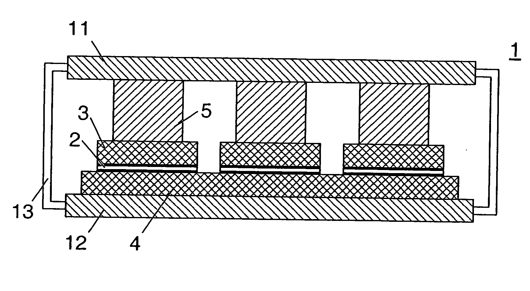
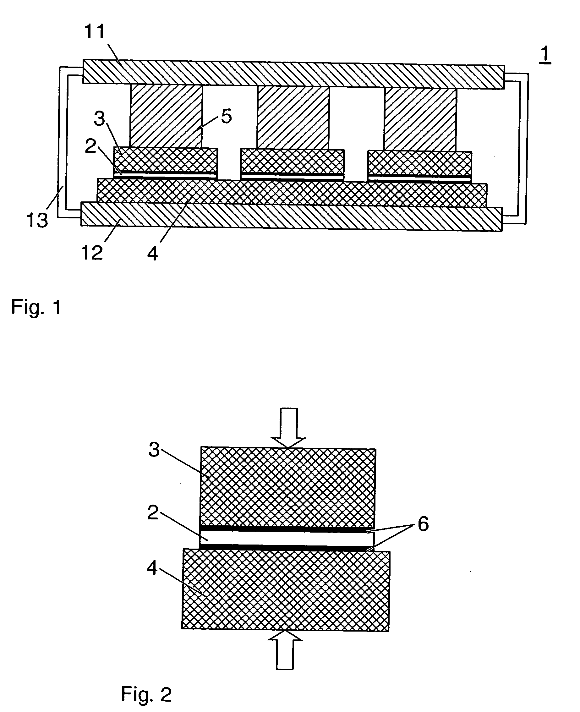
[0023] Referring now to the drawings, FIG. 1 shows a cross section through a preferred exemplary embodiment of a high-power press pack semiconductor module according to the invention. A number of individual Si semiconductor chips 2, e.g. IGBT or Diodes, are arranged isolated and alongside one another in a common housing. These chips are electrically connected in parallel, and the active semiconductor area required for high currents is in this way composed of a large number of individual surfaces. FIG. 1 does not show the normally bonded gate connections for actuating the semiconductor component.

[0024] The Si semiconductor chips 2 have a metallized main electrode on both the top face and bottom face, which make electrical contact with metallic contact surfaces. The chips are mounted on a conductive base plate 4 and a conductive top plate 3 is arranged directly above each chip. A contact piston 5 is pressing the top plate and the Si semiconductor chip against the base plate. The arra...


PUM

PropertyMeasurementUnit
melting pointaaaaaaaaaa
coefficient of thermal expansionaaaaaaaaaa
metallicaaaaaaaaaa

Abstract

The high-power pack semiconductor module (1) comprises a layer (3, 4), which is brought into direct contact with one or both of the main electrodes of the Si semiconductor chip, (2), said layer being made of a metal matrix composite material whose coefficient of thermal expansion can be tailored to a value either close or matching that of Si.

Description

BACKGROUND OF THE INVENTION [0001] The present invention relates to the technical field of power electronics. It concerns a high-power press pack semiconductor module, in particular an IGBT (Insulated Gate Bipolar Transistor) or a Thyristor module. BACKGROUND ART [0002] Press pack modules comprising either Thyristor or IGBT semiconductor devices are used in the field of power electronics for switching applications as in HVDC-converters (high voltage direct current converters). In order to achieve higher blocking voltages than with individual devices press pack modules are stacked in series on top of each other. Pressure is applied to that stack to assure proper electrical and thermal contact between the individual press pack modules. [0003] In case of a defect in one of the pressure-contacted semiconductor devices of such a stack, the Si (silicon) chip of the semiconductor device first melts locally, as current flows, forming a conductive channel (hot spot) over the entire thickness...

Claims


Application Information

Patent Timeline
Patent Type & Authority Applications(United States)
IPC IPC(8): H01L29/73C22C49/06H01L23/051H01L23/48H01L23/492H01L25/07
CPCH01L23/051H01L23/4924H01L2924/1305H01L2924/1301H01L2924/10253H01L2924/01047H01L2924/01006H01L24/29H01L24/72H01L25/072H01L2924/01004H01L2924/01012H01L2924/01013H01L2924/01029H01L2924/01033H01L2924/01042H01L2924/01078H01L2924/01079H01L2924/01082H01L2924/01322H01L2924/01327H01L2924/014H01L2924/13055H01L2924/3011H01L2924/00H01L23/62
Inventor GUNTURI, SATISHSCHNEIDER, DANIEL
Owner HITACHI ENERGY SWITZERLAND AG
Why Eureka
Try Eureka