Junction termination structures for wide-bandgap power devices

Inactive Publication Date: 2006-06-08
MICROSEMI
View PDF13 Cites 31 Cited by
  • Summary
  • Abstract
  • Description
  • Claims
  • Application Information

AI Technical Summary

Benefits of technology

[0009] The present invention is a novel type of termination structure and method of making, which provides a high blocking voltage while being fabricated with a simple controllable process. Features of the invention include the use of a finely patterned structure that provides the desired lateral taper and the combination of resistive a

Problems solved by technology

The intent of these structures is to reduce high electric fields at the edge of the device, resulting in higher blocking voltages.
All these approaches wo

Method used


Image

  • Junction termination structures for wide-bandgap power devices
  • Junction termination structures for wide-bandgap power devices
  • Junction termination structures for wide-bandgap power devices

Examples


Example

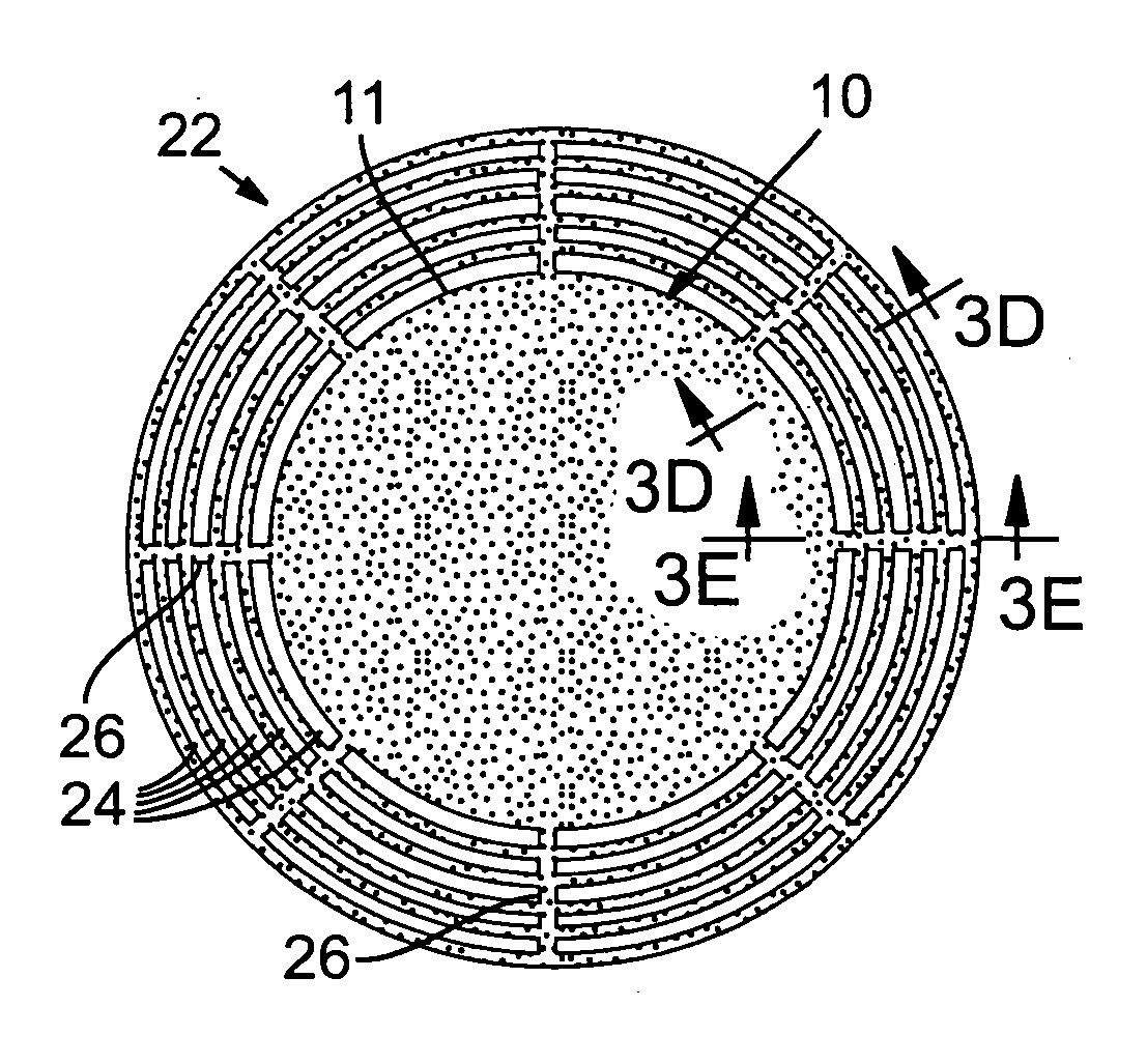
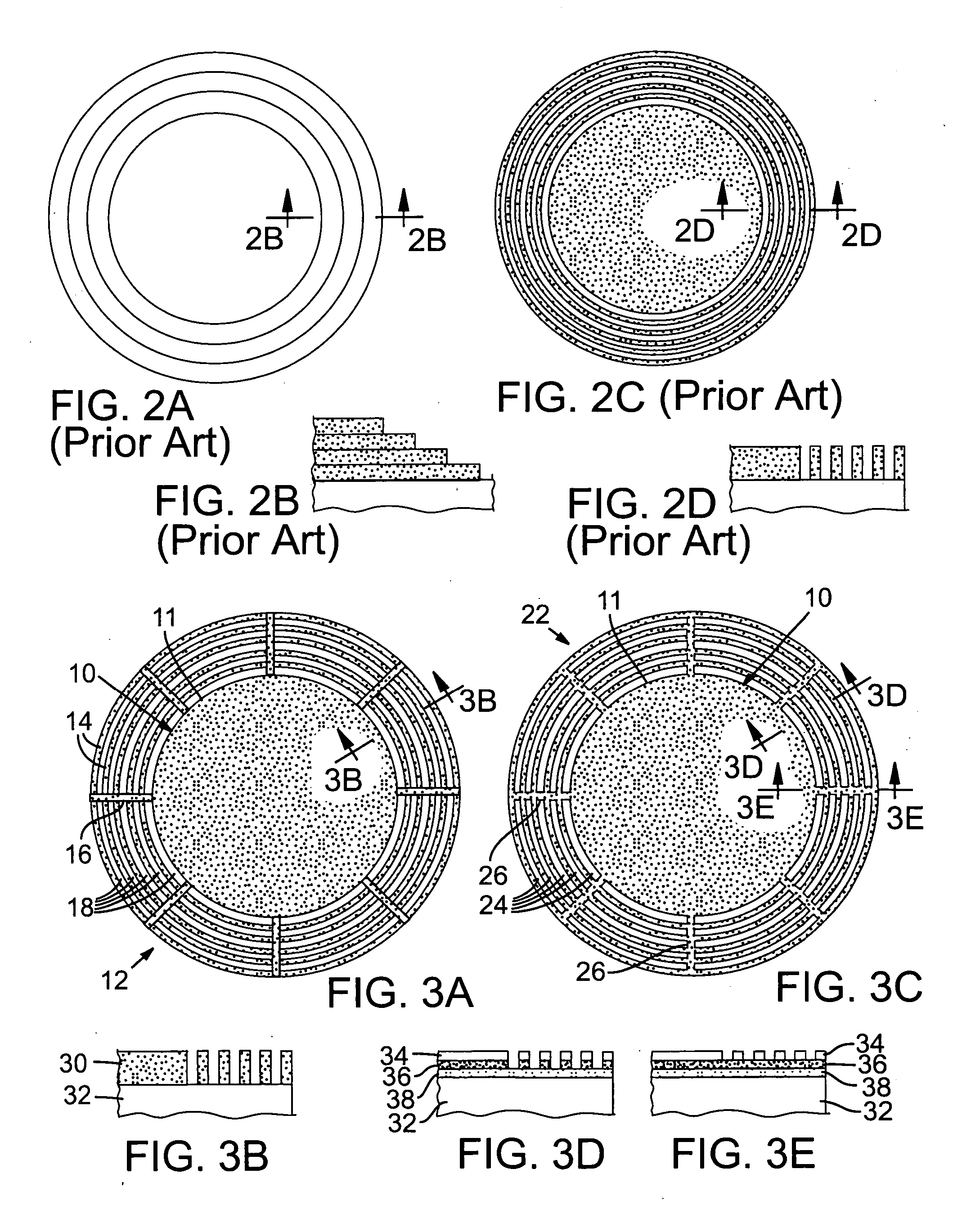
[0024] A junction termination structure for a high voltage semiconductor power device according to various embodiments of the invention comprises a finely patterned structure with different implant doses or different etch depths, that reduce the high field regions in the structure. This approach is increasingly effective as the finely patterned structure can have a minimum feature size that is distinctly smaller than the depletion layer width of the device. An added feature is the use of highly resistive links between concentric rings, potentially combined with regions that cannot be fully depleted and regions that are always depleted. Typical dimensions for SiC blocking layers are 10-micron depletion layers for 1000V blocking voltage, while the edge termination structure would be multiple times the depletion layer width, namely 30 to 100 micron. Structures with higher blocking voltage have larger depletion layers and also larger edge terminations. The desired minimum feature size i...


PUM


Abstract

Disclosed are a variety of junction termination structures for high voltage semiconductor power devices. The structures are specifically aimed at providing a high breakdown voltage while being constructed with a minimal number of process steps. The combination of an RIE etch and/or implantation and anneal process with a finely patterned mesh provides the desired radial gradient for maximum breakdown voltage. The structures provide control of both the conductivity and charge density within the region. These structures can beneficially be applied to all high voltage semiconductor device structures, but are of particular interest for wide bandgap devices as they tend to have very high breakdown fields and scaled dimensions of the depletion layer width.

Description

RELATED APPLICATION DATA [0001] This application claims priority from U.S. provisional application Ser. No. 60 / 631,024, filed Nov. 24, 2004, incorporated by reference herein.STATEMENT REGARDING FEDERALLY SPONSORED RESEARCH OR DEVELOPMENT [0002] This invention was made under National Institute of Standards and Technology, Advanced Technology Programs, U.S. Department of Commerce Cooperative Agreement No. 70NANB 3H3016. The United States Government has certain rights in this invention.BACKGROUND OF THE INVENTION [0003] This invention relates to junction termination structures in high voltage power semiconductor devices and more particularly to junction termination structures for wide bandgap power devices, such as silicon carbide, gallium nitride, gallium aluminum nitride, gallium indium nitride, diamond devices, and the like. [0004] Junction termination structures are a common feature of most high voltage power switching devices, such as p-n diodes or Schottky diodes, and bipolar tra...

Claims


Application Information

Patent Timeline
IPC IPC(8): H01L29/47
CPCH01L29/0611H01L29/0619H01L29/0692H01L29/1608H01L29/73H01L29/861H01L29/872
Inventor ZEGHBROECK, BART VAN
Owner MICROSEMI
Why Eureka
Try Eureka