Semiconductor device, its manufacturing method, and radio communication device

a technology of electromagnetic radiation and semiconductor devices, applied in the direction of basic electric elements, gated amplifiers, gain control, etc., can solve the problems of degrading the connection property of the wire bonding and the imperfect traditional techniques, and achieve the effect of reducing the variation of the inductance of the wire, reducing the efficiency and output of the mobile phon

Active Publication Date: 2006-06-08
MURATA MFG CO LTD
View PDF2 Cites 13 Cited by
  • Summary
  • Abstract
  • Description
  • Claims
  • Application Information

AI Technical Summary

Benefits of technology

[0039] Because the metallized layer extended in the direction for crossing the inner wall of the recess, which is closer to the drain bonding pad, is formed a little shorter than the semiconductor chip, one side of the semiconductor chip can come in contact with the inner wall of the recess, which is closer to the drain bonding pad by the self-alignment action of the bonding material due to its surface tension. Consequently, the drain wire for connecting the drain electrode of the semiconductor chip to the drain bonding pad provided on the surface of the wiring substrate is fixed in length, thereby the wire inductance is fixed. As a result, both output and efficiency of each communication system of the mobile phone in which the semiconductor device in this embodiment is built are fixed, thereby the characteristics of the mobile phone (radio communication device) are stabilized.
[0040] (c) According to the method for manufacturing a semiconductor device in this embodiment, a plurality of recesses are formed in the main surface of the wiring substrate and a metallized layer is formed in the same size as that of the semiconductor chip in each of the recesses so as to reach the inner wall of the recess, which is closer to the drain bonding pad. A fusion bonding material is put on the metallized layer and a semiconductor chip is supplied on the bonding material, then the bonding material is heated and fused temporarily so that the semiconductor chip is positioned and fixed accurately at the bottom of the recess due to the self-alignment action of the fused bonding material. Consequently, the semiconductor chip is fixed so that one side thereof comes in contact with the inner wall of the recess, which is closer to the drain bonding pad. Thus, the drain electrode of the semiconductor chip is always fixed and the drain wire is fixed in length, thereby the variation of the wire inductance is reduced. As a result, both efficiency and output of the mobile phone in which the semiconductor device in this embodiment is built are stabilized.

Problems solved by technology

However, this technique just positions and fixes the semiconductor chip in the recess by inclining the inner wall of the recess and using the inclined plane to move the chip or using a surface tension of a member having the predetermined surface tension, which is inserted between the chip and the side face (inner wall) of the recess.
In such a radio communication device as a mobile phone that is required of high and efficient outputs, however, such conventional techniques have been found imperfect, since the techniques depend only on the performance of such a chip bonding device.
As a result, the connection property of the wire bonding is often degraded.

Method used


Image

  • Semiconductor device, its manufacturing method, and radio communication device
  • Semiconductor device, its manufacturing method, and radio communication device
  • Semiconductor device, its manufacturing method, and radio communication device

Examples


first embodiment

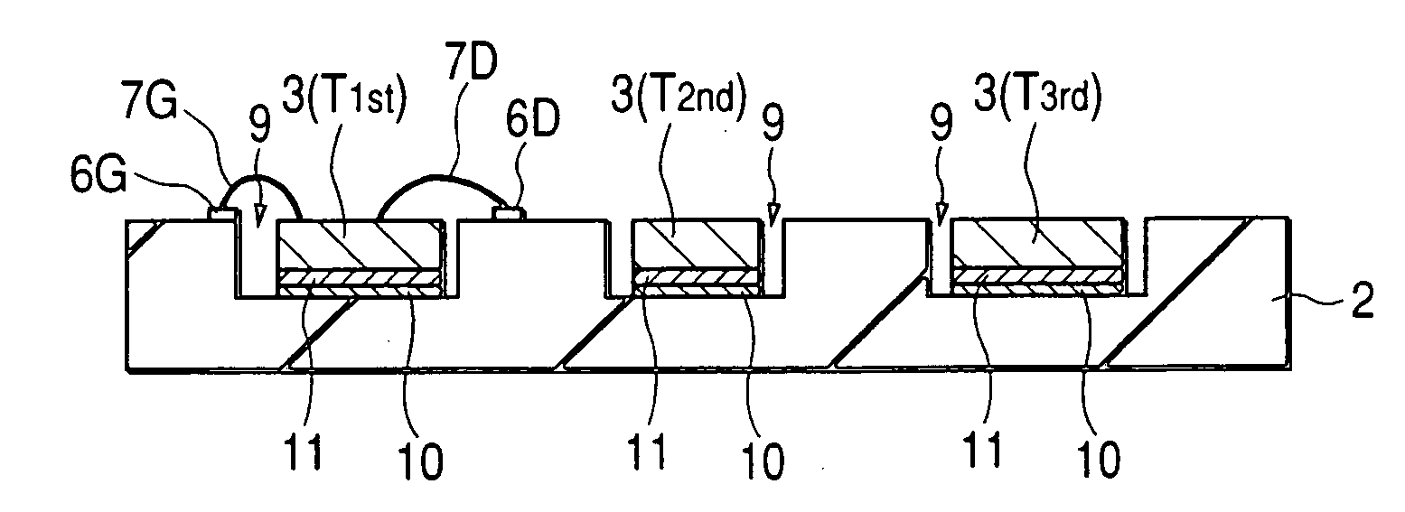
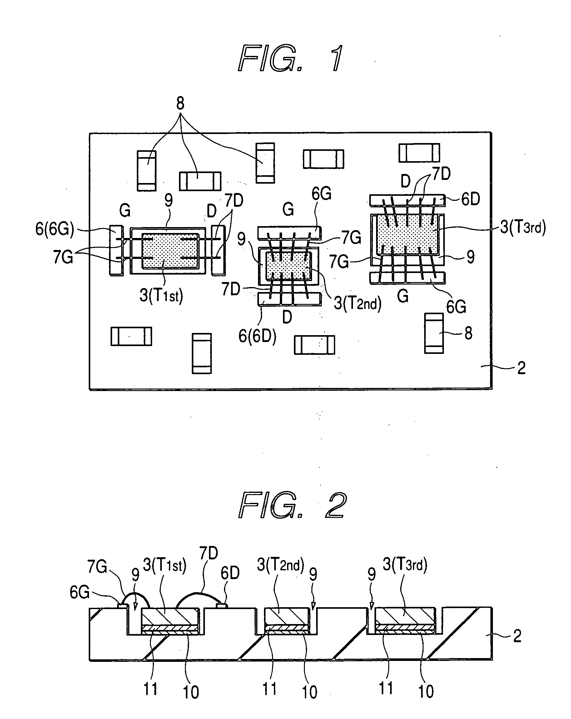
[0067]FIGS. 1 through 15 relate to a semiconductor device (high frequency power amplification unit) including a multistage amplifier unit built therein, its manufacturing method, and a radio communication device (mobile phone) including the semiconductor device built therein in an embodiment (first embodiment) of the present invention.

[0068] At first, the semiconductor device that includes a multistage amplifier unit and its manufacturing method of the present invention will be described with reference to FIGS. 1 through 9 before describing the dual band high frequency power amplification unit and the mobile phone (radio communication device) of the present invention.

[0069] As shown in FIG. 1, the semiconductor device 1 in which a multistage amplifier unit is built includes various types of electronic parts mounted on the main surface of its module substrate 2 configured by a wiring substrate. Although this module substrate is not shown in FIG. 1, the main surface is capped to fun...

second embodiment

[0138]FIGS. 16 through 18 show illustrations related to a high frequency power amplification unit in another (the second) embodiment of the present invention. FIG. 16 is a top view of a layout of electronic parts mounted on the module substrate of the high frequency power amplification unit. FIG. 17 is a bottom view of the module substrate and FIG. 18 is a circuit diagram of the high frequency power amplification unit.

[0139] Just like the first embodiment, the high frequency power amplification unit 1 in this second embodiment includes multistage amplifier units for both GSM and DCS communication systems. However, the high frequency power amplification unit 1 in this second embodiment, as shown in FIGS. 16 through 18, has an input terminal (Pin) common to both GSM and DCS communication systems, so that the unit 1 is configured as a 2-input terminal and 2-output terminal unit.

[0140] As shown in FIG. 16, a / Vct1 terminal (1), a Vct1 terminal (2), a ground terminal (GND), a Vdd2 term...

third embodiment

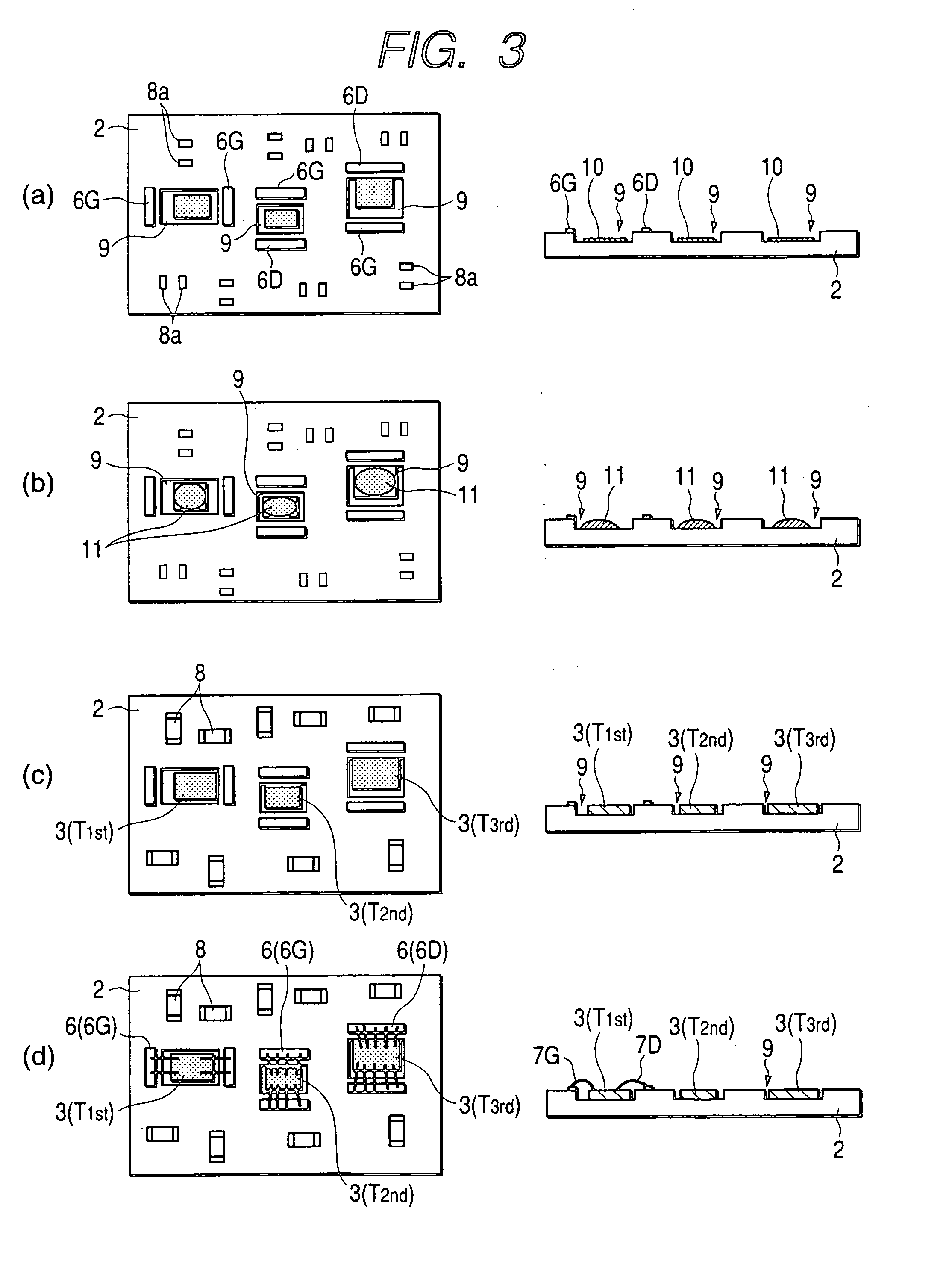
[0147]FIG. 19 is a block diagram of a high frequency power amplification unit in the third embodiment of the present invention. In this third embodiment, each semiconductor chip 3 is positioned and fixed in a square recess 9 with respect to two adjacent sides of the recess 9 formed in the main surface of the module substrate 2. Those two sides are used as references for the positioning and fixing. The corresponding two sides (left and upper sides in FIG. 19) of the semiconductor chip 3 come in contact with those two sides (left and upper sides in FIG. 19) of the recess 9. In this example, a hetero bipolar transistor (HBT) is used as the transistor, that is, an amplifier.

[0148] In this third embodiment, as shown in FIGS. 21A and 21B, each semiconductor chip 3 is fixed at the bottom of a recess 9. FIGS. 21A and 21B are explanatory views of how the semiconductor chip 3 that includes the final stage transistor will become before and after it is fixed in the recess 9. FIG. 21A shows the...


PUM


Abstract

The variation of the parasitic inductance generated at the output terminal of a transistor in the final stage of a multistage amplifier unit is reduced. One side of the semiconductor chip that includes the final stage transistor is put in contact with the inner wall of a square recess formed in a wiring substrate. The semiconductor chip is positioned and fixed accurately at the bottom of the recess, whereby the drain wire of the transistor is fixed. Then, a chip edge at which the drain electrode is disposed on top of the chip is put in contact with the inner wall of the recess, which is closer to the drain bonding pad. A metallized layer is formed of the same size as that of the chip at the bottom of the recess and a fusion bonding material is supplied on the metallized layer.

Description

TECHNICAL FIELD [0001] The present invention relates to a semiconductor device, its manufacturing method, and a radio communication device, more particularly to a technique applicable effectively to a multistage amplifier unit (high frequency power amplification unit: high frequency power amplification module) configured by a plurality of semiconductor amplification elements connected serially in a plurality of stages and such a radio communication device as a mobile phone in which the high frequency power amplification unit is built. BACKGROUND ART [0002] A high frequency power amplification unit employed for such a radio communication device as a car telephone, mobile phone, or the like is configured by a plurality of amplifiers, each being configured by a transistor (semiconductor amplification element) and connected to another serially. Usually, two or three of such amplifiers are disposed in a plurality of amplification stages. The amplifier in the last stage (final amplificati...

Claims


Application Information

Patent Timeline
Patent Type & Authority Applications(United States)
IPC IPC(8): H01L23/48H01L23/52H01L23/34H01L21/60H01L23/13H01L23/66H01L25/065
CPCH01L2224/48647H01L2224/48639H01L2924/13055H01L2924/12041H01L2924/13064H01L2924/1306H01L2924/1305H01L23/13H01L23/66H01L24/06H01L24/29H01L24/45H01L24/49H01L24/83H01L24/85H01L25/0655H01L2223/6644H01L2224/05553H01L2224/05639H01L2224/05647H01L2224/291H01L2224/32225H01L2224/45015H01L2224/45144H01L2224/48091H01L2224/48227H01L2224/49113H01L2224/49171H01L2224/49175H01L2224/73265H01L2224/81143H01L2224/83192H01L2224/83801H01L2224/85H01L2224/92247H01L2924/01002H01L2924/01005H01L2924/01006H01L2924/01014H01L2924/01015H01L2924/01029H01L2924/01032H01L2924/01033H01L2924/01047H01L2924/01074H01L2924/01078H01L2924/01079H01L2924/01082H01L2924/014H01L2924/09701H01L2924/10329H01L2924/14H01L2924/15151H01L2924/15153H01L2924/15165H01L2924/1517H01L2924/15313H01L2924/19041H01L2924/19042H01L2924/19043H01L2924/19105H01L2924/20752H01L2924/30105H01L2924/30107H01L2924/3011H01L2924/3025H01L24/32H01L24/48H01L2924/00014H01L2224/29101H01L2924/0132H01L2224/78H01L2924/00H01L2924/01031H01L2924/00012H01L2224/85205H01L2224/0401H01L24/73H01L2224/05554H01L2924/10161H01L2224/75745H03F3/245H03F3/72H03F2200/111
Inventor IDA, TSUTOMUKOBAYASHI, YOSHIHIKOHASHIZUME, MASAKAZUSHIOKAWA, YOSHINORIKIKUCHI, SAKAE
Owner MURATA MFG CO LTD
Why Eureka
Try Eureka