Thermal management of surface-mount circuit devices

a surface-mount circuit device and thermal management technology, applied in the direction of printed circuit aspects, electrical apparatus construction details, printed circuit association, etc., can solve the problems that the thermal management of metal-containing ceramic layers cannot be improved by the use of metal-containing ceramic layers, and the ltcc substrate is also electrically conductive, etc., to achieve the effect of improving thermal managemen

Active Publication Date: 2006-06-08
DELPHI TECH IP LTD
View PDF18 Cites 49 Cited by
  • Summary
  • Abstract
  • Description
  • Claims
  • Application Information

AI Technical Summary

Benefits of technology

[0007] The present invention provides a circuit board assembly having a laminate construction, such as an LTCC ceramic substrate. The substrate is...

Problems solved by technology

However, a limitation of this approach is that the resulting metal-containing layers of the LTCC substrate are also electrically conductive to some degree.
Because of the circuit components and their associated interconnect vias within the LTCC substrate, improved thermal conductivity cannot be obtained by the use of metal-containing ceramic layers.
While able to promote the conduction of heat away from power devices, thermal vias incur additional processing and material costs, reduce routing density, and can limit design flexibility.
Furthermore, thermal vias may be inadequate to achieve suitable thermal management of certain power devices, particularly devices of the flip-chip type.
For example, therm...

Method used


Image

  • Thermal management of surface-mount circuit devices
  • Thermal management of surface-mount circuit devices
  • Thermal management of surface-mount circuit devices

Examples


first embodiment

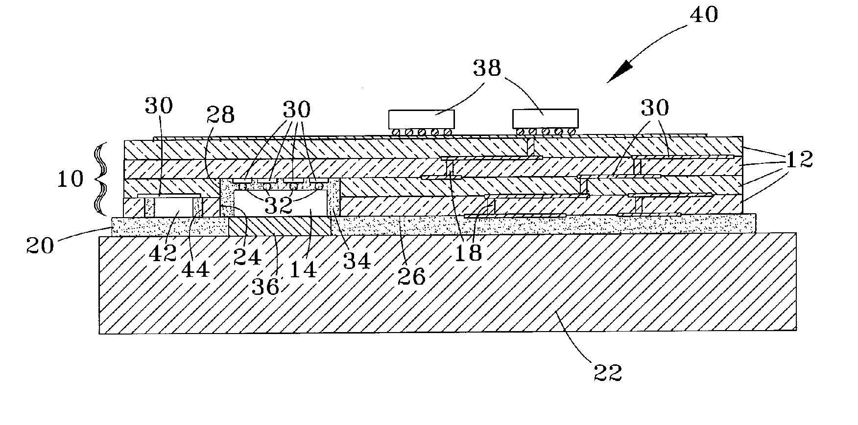
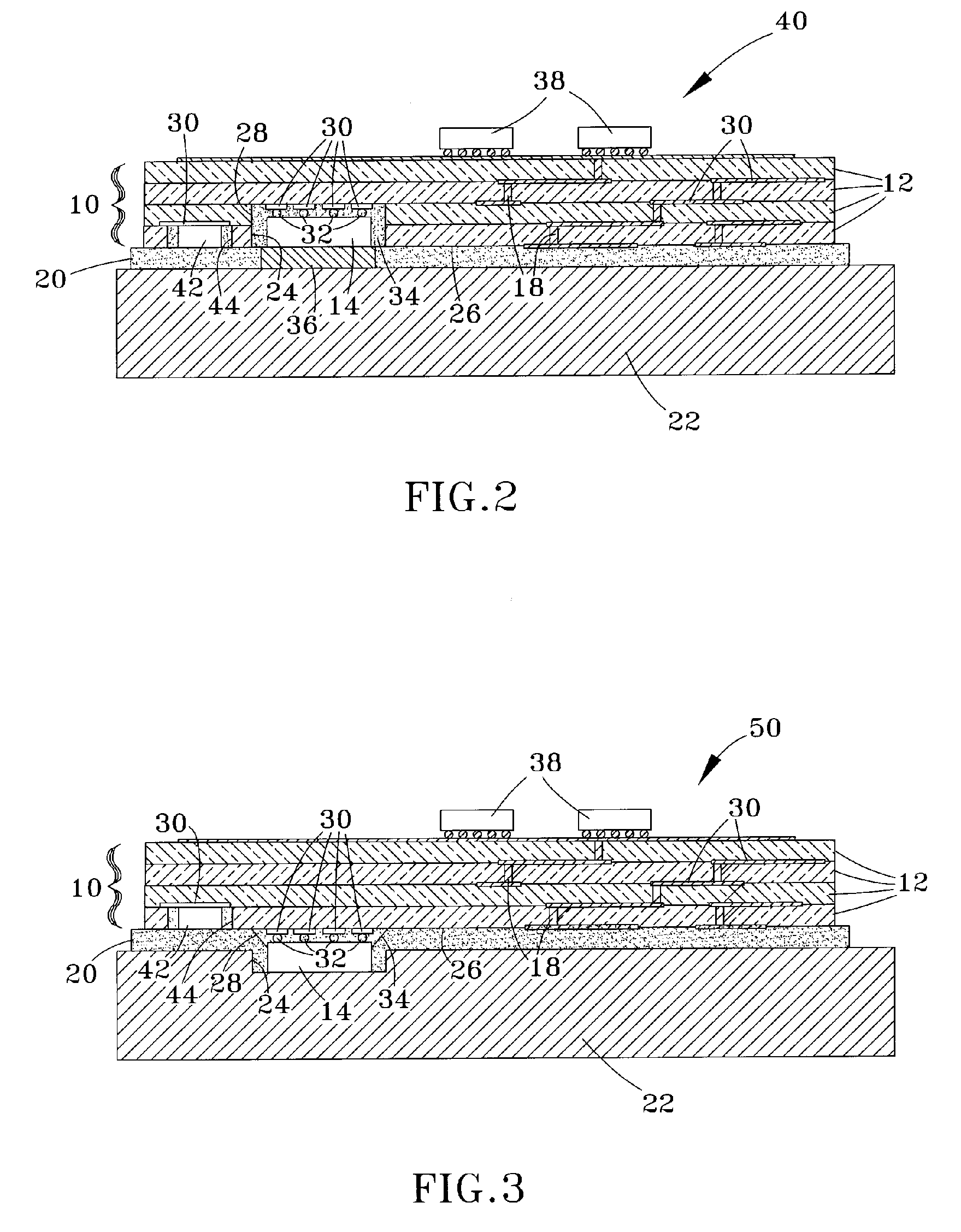
[0014]FIG. 2 depicts a circuit board assembly 40 in which a power flip chip 14 is mounted on a low-temperature co-fired ceramic (LTCC) substrate 10 in accordance with the present invention. While a circuit board assembly comprising an LTCC substrate 10 is preferred, the use of other laminate substrates, for example, organic circuit board substrate materials such as FR-4, is also within the scope of this invention.

[0015] As an LTCC, the substrate 10 is a monolithic structure made up of multiple ceramic layers 12 bonded to each other, with thick-film conductors 30 located within the substrate 10 between adjacent layers 12. As with known LTCC processes, the substrate 10 is fabricated using individual green tapes on which the thick-film conductor pastes are deposited which, after stacking and firing at a temperature of, for example up to about 900° C., form the ceramic layers 12 and conductors 30, respectively. Other passive circuit components, such as resistors and capacitors, may also...

second embodiment

[0023]FIG. 3 depicts a circuit board assembly 50 in accordance with the invention in which, for convenience, corresponding components are identified with the same reference numbers as those used in FIG. 2. As such, a power flip chip 14 is mounted on an LTCC substrate 10 made up of multiple ceramic layers 12. The embodiment of FIG. 3 primarily differs from FIG. 2 by its location of the cavity 24 within the heat sink 22 instead of the substrate 10. Multiple solder bumps 32 on the active frontside of the chip 14 electrically and physically attach the chip 14 to conductors 30 on the surface 26 of the substrate 10. The non-active backside of the chip 14 may be bonded to the bottom of the cavity 24 with solder (not shown) or a portion of the adhesive 20 that bonds the heat sink 22 to the substrate 10. An advantage of this embodiment is that heat transfer occurs vertically from the chip 14 to the heat sink 22, as well as laterally into the heat sink 22 through the walls of the cavity 24.

[0...


PUM


Abstract

A circuit board assembly having a laminate construction of multiple layers, such as a LTCC ceramic substrate, with conductor lines between adjacent pairs of layers. A heat sink is bonded to a first surface of the substrate, and a cavity is defined by and between the heat sink and the substrate such that a base wall of the cavity is defined by one of the layers with conductor lines thereof being present on the base wall. A surface-mount circuit device is received within the cavity, mounted to the base wall, and electrically connected to the conductor lines on the base wall. The device is received within the cavity such that a surface of the device contacts a surface region of the heat sink. The surface of the device is bonded to the surface region of the heat sink to provide a substantially direct thermal path from the device to the heat sink.

Description

BACKGROUND OF THE INVENTION [0001] The present invention generally relates to thermal management of electronic circuit components. More particularly, this invention relates to a circuit board-heat sink structure with an interior cavity containing a surface-mount device thermally coupled to the heat sink to provide enhanced thermal management of the device. [0002] A variety of approaches are known for dissipating heat generated by semiconductor devices, such as integrated circuit (IC) chips. One method is to use a flex circuit laminated or bonded to a heat sink. If the flex circuit material is sufficiently thin, this approach can employ a highly conductive path formed by plated vias through the flex circuit to the heat sink. Another method is to equip a printed circuit board (PCB) with an innerlayer heat sink that is the same size or larger than the PCB to provide a large heat sink for the entire board, and rely on conduction through the PCB material to the heat sink beneath. High-po...

Claims


Application Information

Patent Timeline
IPC IPC(8): H05K7/06H05K7/20
CPCH01L23/13H01L23/36H01L23/367H01L23/3675H01L23/5389H01L24/48H01L25/16H01L2224/16H01L2224/16225H01L2224/32225H01L2224/4847H01L2224/73265H01L2924/00011H01L2924/00014H01L2924/01087H01L2924/09701H01L2924/14H01L2924/19041H01L2924/19107H05K1/021H05K1/0306H05K1/183H05K3/0061H05K3/4611H05K3/4629H05K2201/09745H05K2201/1056H01L2924/00H01L2224/0401H01L2224/45099H01L2224/45015H01L2924/207
Inventor FAIRCHILD, MANUELZIMMERMAN, DAVIDCHENGALVA, SURESH
Owner DELPHI TECH IP LTD
Why Eureka
Try Eureka