
Field-effect transistor, sensor using it, and production method thereof

a field-effect transistor and sensor technology, applied in the field of field-effect transistors, can solve the problems of difficult to make biomolecules carried into the pores in high density, difficult to control the diameter of the pores, etc., and achieve the effect of raising the sensitivity of the sensor, reducing the cost of production, and improving the stability of the structur

Inactive Publication Date: 2006-06-08
CANON KK
View PDF32 Cites 10 Cited by
  • Summary
  • Abstract
  • Description
  • Claims
  • Application Information

AI Technical Summary

Benefits of technology

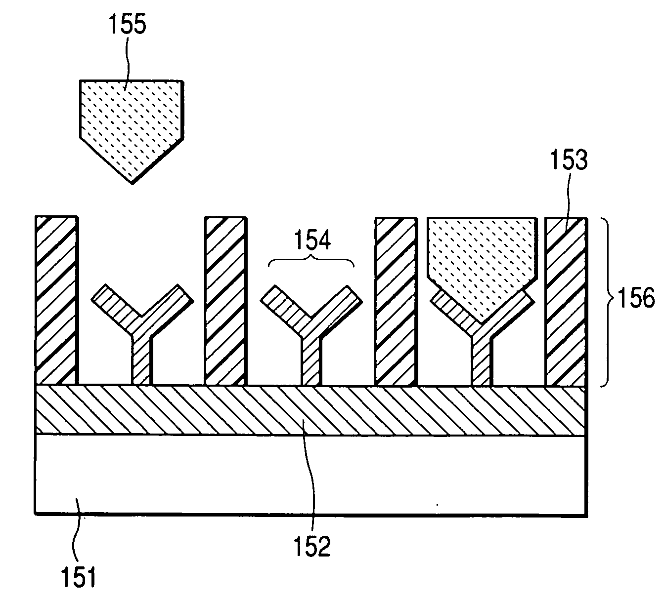
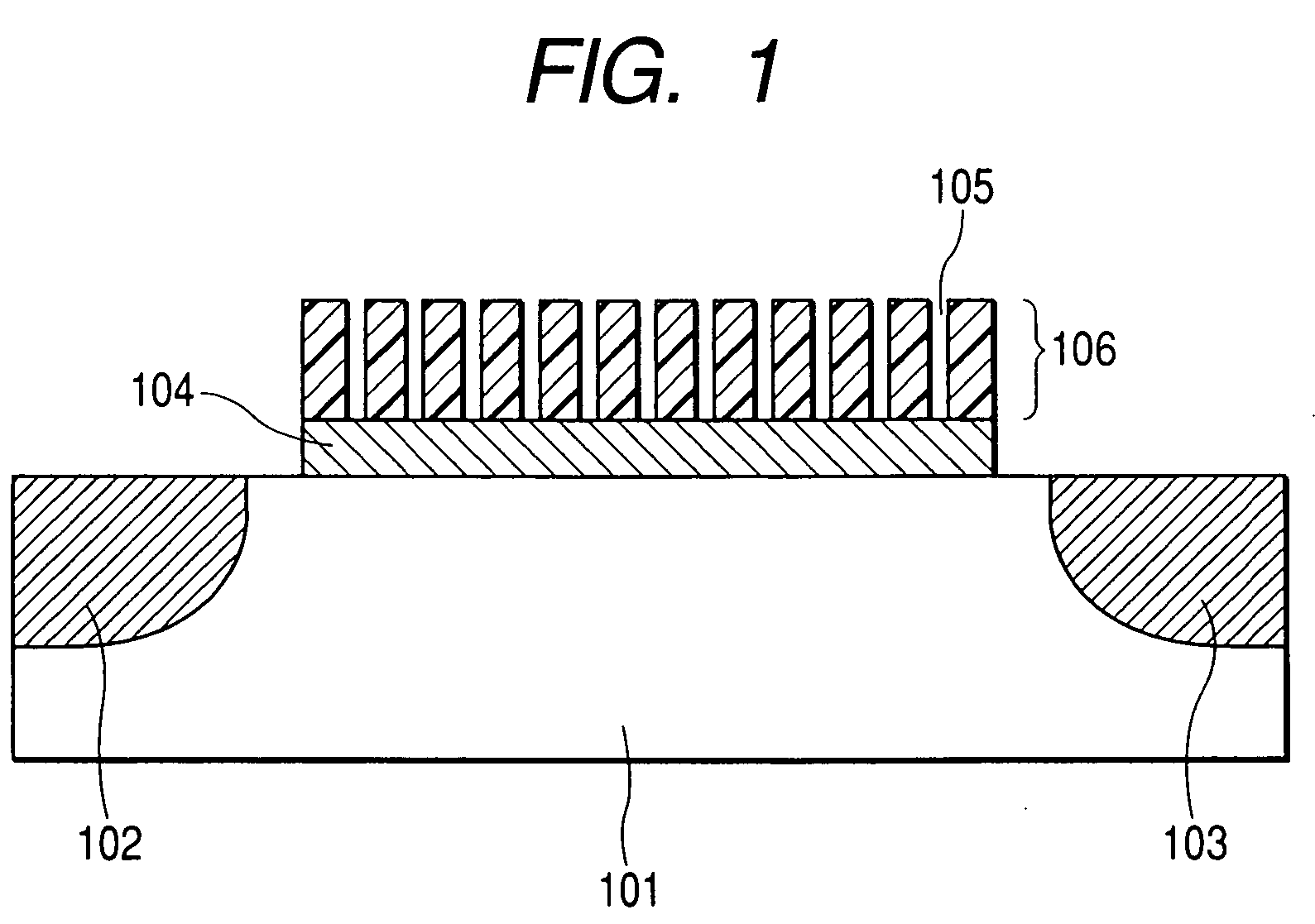
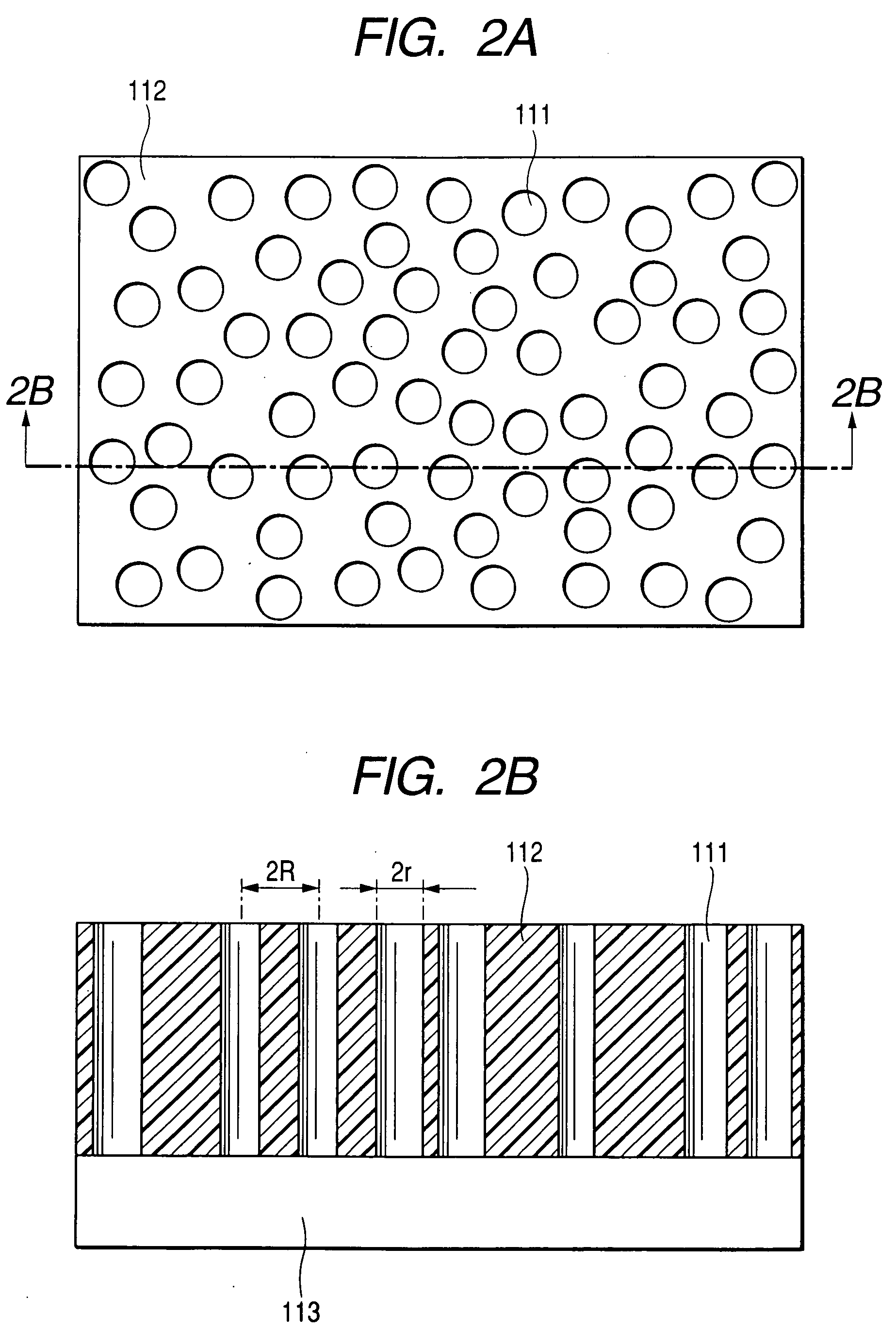
[0004] Then, the present invention provides a field-effect transistor, and a sensor using it, the field-effect transistor which has high measuring sensitivity and is excelled in response by forming a porous film in the sensitive section of the field-effect transistor, the porous film which has cylindrical pores which are perpendicular to a substrate, and have high pore density and 20 nm or less of pore diameter.
[0019] In addition, the present invention can provide a production method which can simply produce the above-mentioned sensor in low cost.

Problems solved by technology

Nevertheless, in a conventional method, as shown in FIG. 9, since the structure in a nano meter level is formed by material particles (clusters) being implanted into the sensitive section of the sensor, it is very hard to control the shape of the structure so as to mostly coincide with the contour shape of the outside of the biogenic substance.
In addition, although it is shown that it is possible to produce a porous layer, it is very hard to control the diameter of its pores, its pore density, etc., and it is very difficult to make biomolecules carried into the pores in high density.
Furthermore, depending on a formation method, there is a possibility of making a defect and the like arise in the sensor sensitive sections (gate insulating film etc.) and reducing the measuring sensitivity.

Method used


Image

  • Field-effect transistor, sensor using it, and production method thereof
  • Field-effect transistor, sensor using it, and production method thereof
  • Field-effect transistor, sensor using it, and production method thereof

Examples


example 1

[0061] This example shows the case that a sensor having a porous film, having pores which is perpendicular to a substrate and has a cylindrical shape, on a sensitive section (a gate insulating film) of a field-effect transistor is used as a gas sensor. Here, although the case that a main component except oxygen is silicon as a material which constitutes the porous film is shown, it is possible to adapt almost similar sensor structure, production method, and effects also in the case that a main component except oxygen is germanium or a composite of silicon and germanium.

[0062] First, as shown in FIG. 6A, a 50-nm-thick silicon oxide film (a gate oxide film) is formed on a p-type single crystal silicon substrate by the thermal oxidation method. Next, an about 200-nm-thick aluminum silicon mixing film including 50 atomic % of aluminum to the whole amount of aluminum and silicon was formed on the silicon oxide, which is a gate insulating film, by using the magnetron sputtering method as...

example 2

[0069] This example shows the case that a sensor having a porous film, having pores which are perpendicular to the substrate and has cylindrical shapes, on a sensitive section (a gate insulating film) of a field-effect transistor is used as a biosensor. Here, the case that a main component which constitutes the porous film is a silicon oxide will be shown.

[0070] First, as shown in FIG. 6A, a 50-nm-thick silicon oxide film (a gate oxide film) is formed on a p-type single crystal silicon substrate by the thermal oxidation method. Next, an about 100-nm-thick aluminum silicon mixing film including 60 atomic % of aluminum to the whole amount of aluminum and silicon was formed on a gate insulating film, which was a sensitive section, by using the magnetron sputtering method. A circular aluminum silicon-mixing target with the diameter of 4 inches (101.6 mm) was used as a target. What aluminum powder and silicon powder were sintered at a ratio of 60 atomic %: 40 atomic % was used as the al...

example 3

[0079] This example shows the case that a sensor having a porous film, having pores which are perpendicular to a substrate and have cylindrical shapes, on a sensitive section (a gate insulating film) of a field-effect transistor is used as a pH sensor measuring pH of an acid and alkali solutions. Here, although the case that a material which constitutes the porous film is silicon except oxygen is shown, it is possible to adapt almost similar sensor structure, production method, and effects also in the case of germanium or a composite of silicon and germanium.

[0080] First, as shown in FIG. 6A, a 50-nm-thick silicon oxide film (a gate oxide film) is formed on a p-type single crystal silicon substrate by the thermal oxidation method. Next, on the silicon oxide film, an about 200-nm-thick aluminum silicon mixing film including 50 atomic % of aluminum to the whole amount of aluminum and silicon was formed on the silicon oxide, which is a gate insulating film, by using the magnetron sput...


PUM

PropertyMeasurementUnit
pore diameteraaaaaaaaaa
pore sizeaaaaaaaaaa
diameteraaaaaaaaaa

Abstract

A sensor which has high measuring sensitivity and is excellent in response is provided by forming a porous film in a sensitive section of a field-effect transistor. It comprises a porous body, which is formed on a sensitive section (here, a gate insulating film) of the field-effect transistor and has cylindrical pores which are formed almost perpendicularly to a substrate, and the field-effect transistor. It uses as a porous film a porous film which is made of a semiconductor material whose main component (except oxygen) is silicon, germanium, or a composite of silicon and germanium, or a porous film made of an insulation material whose main component is silicon oxide, which has pores perpendicular to the substrate.

Description

TECHNICAL FIELD [0001] The present invention relates to a field-effect transistor using a porous film which has pores with a cylindrical shape vertical to a substrate on a sensitive section (gate insulating film etc.) of the field-effect transistor, and a sensor using it, and in particular, relates to a sensor, which transduces a chemical or physical change into an electric change, such as a gas sensor detecting a gas (gas molecules etc.), a biosensor detecting a biomaterial such as protein, or a pH sensor detecting pH in a solution. BACKGROUND ART [0002] Up to now, sensors using a field-effect transistor have been known widely (Japanese Patent Application Laid-Open No. S56-76043). Among them, plenty of attempts to enhance measuring sensitivity to a detection object material by forming a nano structure on a sensitive section of a field-effect transistor have been done. For example, a sensor is disclosed, the sensor in which a nano structure (a structure constituted by a plurality of...

Claims


Application Information

Patent Timeline
Patent Type & Authority Applications(United States)
IPC IPC(8): G01N33/00G01N27/414H01L29/78H01L29/786
CPCG01N27/4146Y10T436/11Y10T436/114165Y10S438/96
Inventor FUKUTANI, KAZUHIKOYONEHARA, TAKAOMIYATA, HIROKATSUISHIDA, YOUHEIDEN, TOHRU
Owner CANON KK
Learn More