Imaging systems and methods including an alternating pixel arrangement

a technology of alternating pixel and image sensor, applied in the field can solve the problems of limited signal-to-noise ratio of image sensor array, increase of voltage difference between adjacent pixels, electronic noise, etc., and achieve the effect of reducing capacitance, reducing noise sources, and reducing data line capacitance proportionally

Inactive Publication Date: 2006-06-22
PALO ALTO RES CENT INC
View PDF4 Cites 5 Cited by
  • Summary
  • Abstract
  • Description
  • Claims
  • Application Information

AI Technical Summary

Benefits of technology

[0013] By reducing the number of crossovers between data and ground lines, the data line capacitance may be reduced proportionally. This reduction in capacitance will reduce the noise sources described above, thus improving the signal-to-noise ratio of the imager.

Problems solved by technology

In general, the signal-to-noise ratio of an image sensor array is limited by the electronic noise generated in the array, particularly for imaging conditions when the X-ray dose is low.
There are a number of sources of this electronic noise in an image sensor array.
In addition, the voltage difference on adjacent pixels increases, which might cause leakage between adjacent pixels.
Crystalline silicon, in contrast, would need to be thick and would not have sufficient intrinsic capacitance.
For direct-detection, however, the absorption of length of x-rays in the clinically useful energy range is large even for high-atomic number materials.
Consequently, the intrinsic capacitance of the photoconductor is unlikely to be sufficient.
If the ground connection is disposed parallel to the data connections, glitches from the switching signal may couple onto the sensor, introducing additional line-correlated noise.

Method used


Image

  • Imaging systems and methods including an alternating pixel arrangement
  • Imaging systems and methods including an alternating pixel arrangement
  • Imaging systems and methods including an alternating pixel arrangement

Examples


Embodiment Construction

[0021] The invention relates to imaging systems and sensors that may include an alternating pixel arrangement. For reasons of convenience, the examples below will be discussed using a medical X-ray imaging system. However, it should be appreciated by one skilled in the art that the systems and methods of the invention may be used with any known imaging system without departing from the spirit and scope of the invention.

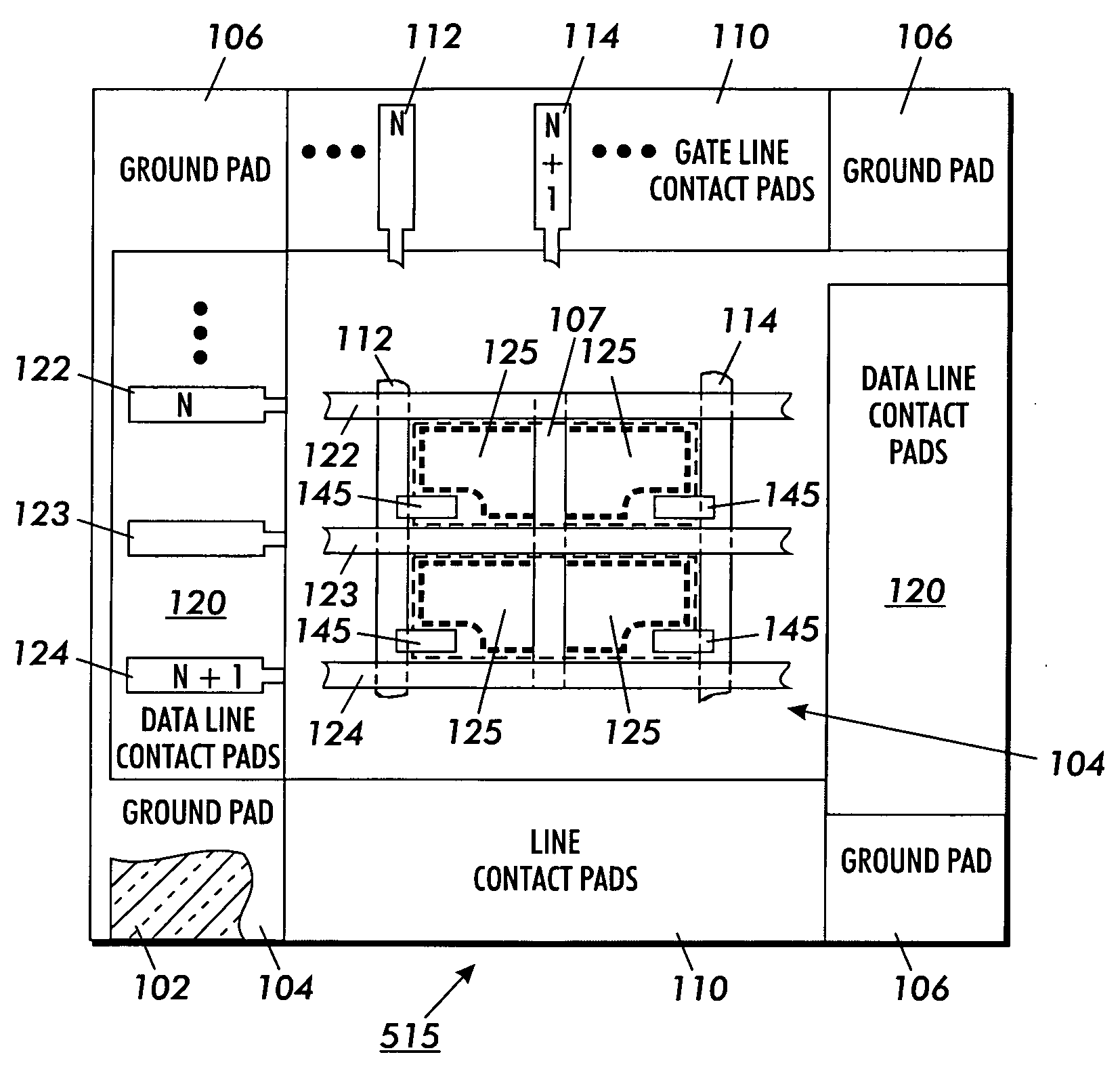
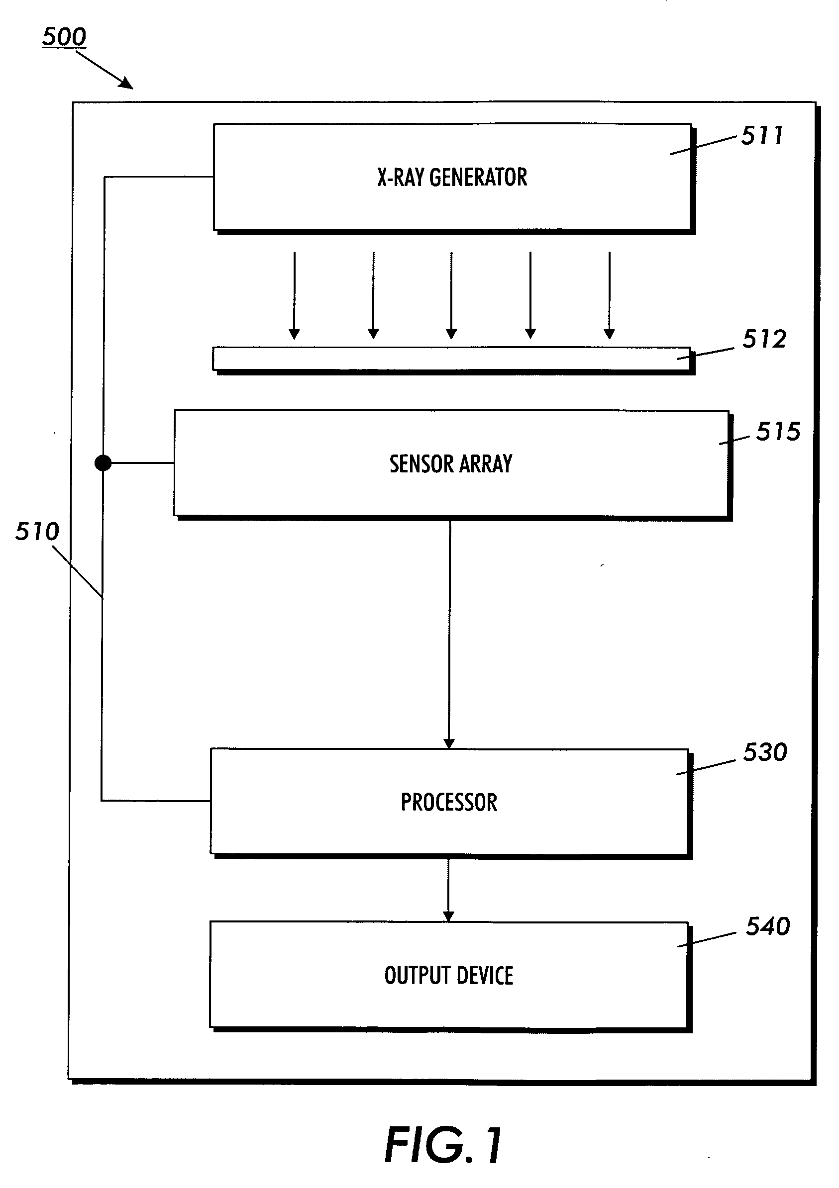
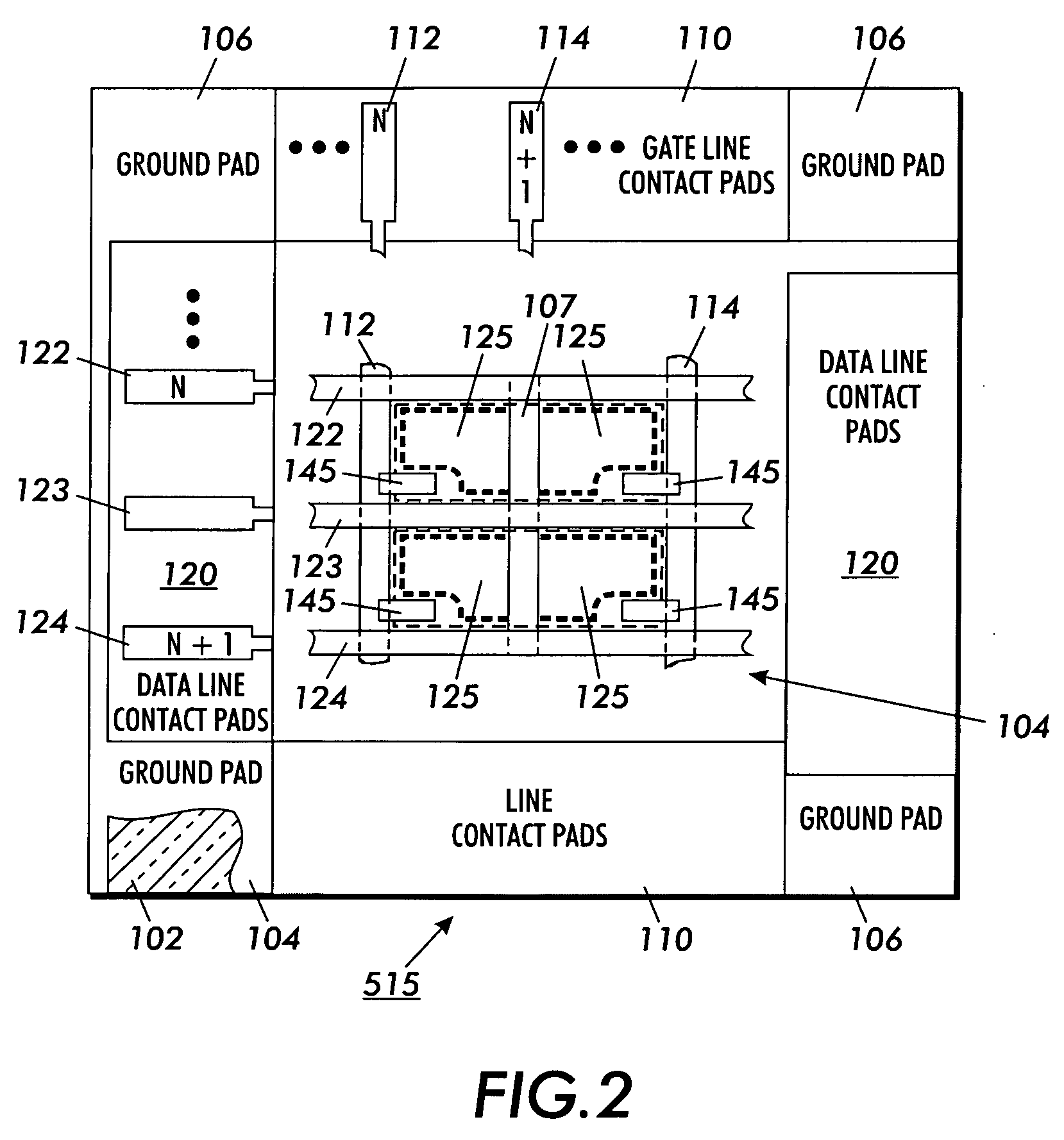
[0022]FIG. 1 is an exemplary diagram showing an imaging system 500 in accordance with the invention. As shown in FIG. 1, the imaging system 500 may include an X-ray generator 510, sensor array 515, controller 530 and output device 540 which may all be connected via links 550. The X-ray generator 510 may be any device that is controlled by the processor 530 to generate X-rays towards the sensor array 515 to capture an image of an object 512. The sensor array 515 may include several layers of material that form the cell circuitry. The sensor array 515 may be any device...


PUM


Abstract

An imaging system includes a plurality of gate lines, a plurality of data lines, a common ground line, a plurality of capacitors and an array of pixels that are alternately arranged so that the common ground line is shared by the plurality of capacitors and shared by at least two rows or columns of pixels. A method of forming an array of pixels in an imaging system includes forming a plurality of gate lines, forming a plurality of data lines, forming a common ground line, forming a plurality of capacitors and forming the array of pixels to be alternately arranged so that the common ground line is shared by the plurality of capacitors and shared by at least two rows of pixels.

Description

BACKGROUND OF THE INVENTION [0001] 1. Field of Invention [0002] The invention relates to imaging systems and methods. More specifically, the invention relates to imaging systems and methods that may include an alternating pixel arrangement. [0003] 2. Description of Related Art [0004] Two-dimensional amorphous silicon (A—Si:H) sensor arrays are well-known devices for real time imaging of incident high energy radiation (see R. A. Street et al., “Large Area Image Sensor Arrays”, in Technology and Applications of Amorphous Silicon, Editor R. A. Street, Springer Series in Materials Science 37, Springer-Verlag, Berlin, 2000, chapter 4, p. 147, for a general description of the structure of the arrays). Such sensor arrays are particularly advantageous for X-ray imaging because they present a relatively large size image sensor array. Each sensor operates on the principal of integrating a charge representative of the quantities of ionizing radiation incident on the sensor. In the direct detec...

Claims


Application Information

Patent Timeline
Patent Type & Authority Applications(United States)
IPC IPC(8): G01T1/24
CPCG01T1/24H01L27/14658H01L27/14692
Inventor RAHN, JEFFREY T.
Owner PALO ALTO RES CENT INC
Why Eureka
Try Eureka