Package for semiconductor device

a semiconductor device and packaging technology, applied in the direction of acceleration measurement using interia forces, acceleration measurement in multiple dimensions, instruments, etc., can solve the problems of difficult to provide a thinner ceramic plate, difficult to reduce the overall thickness of the package, and the ceramic plate may warp or crack, etc., to achieve excellent printing properties and thin packaging

Inactive Publication Date: 2006-06-22
LAPIS SEMICON CO LTD
View PDF1 Cites 1 Cited by
  • Summary
  • Abstract
  • Description
  • Claims
  • Application Information

AI Technical Summary

Benefits of technology

[0013] An object of the present invention is to provide a thinner package for a s

Problems solved by technology

(1) If the thickness of a ceramic plate is less than 0.2 mm, the ceramic plate may warp or crack.
For this reason, it is difficult to provide a thinner ceramic plate, and making it difficult to reduce the overall thickness of the package.
This leads to a dem

Method used


Image

  • Package for semiconductor device
  • Package for semiconductor device
  • Package for semiconductor device

Examples


first embodiment

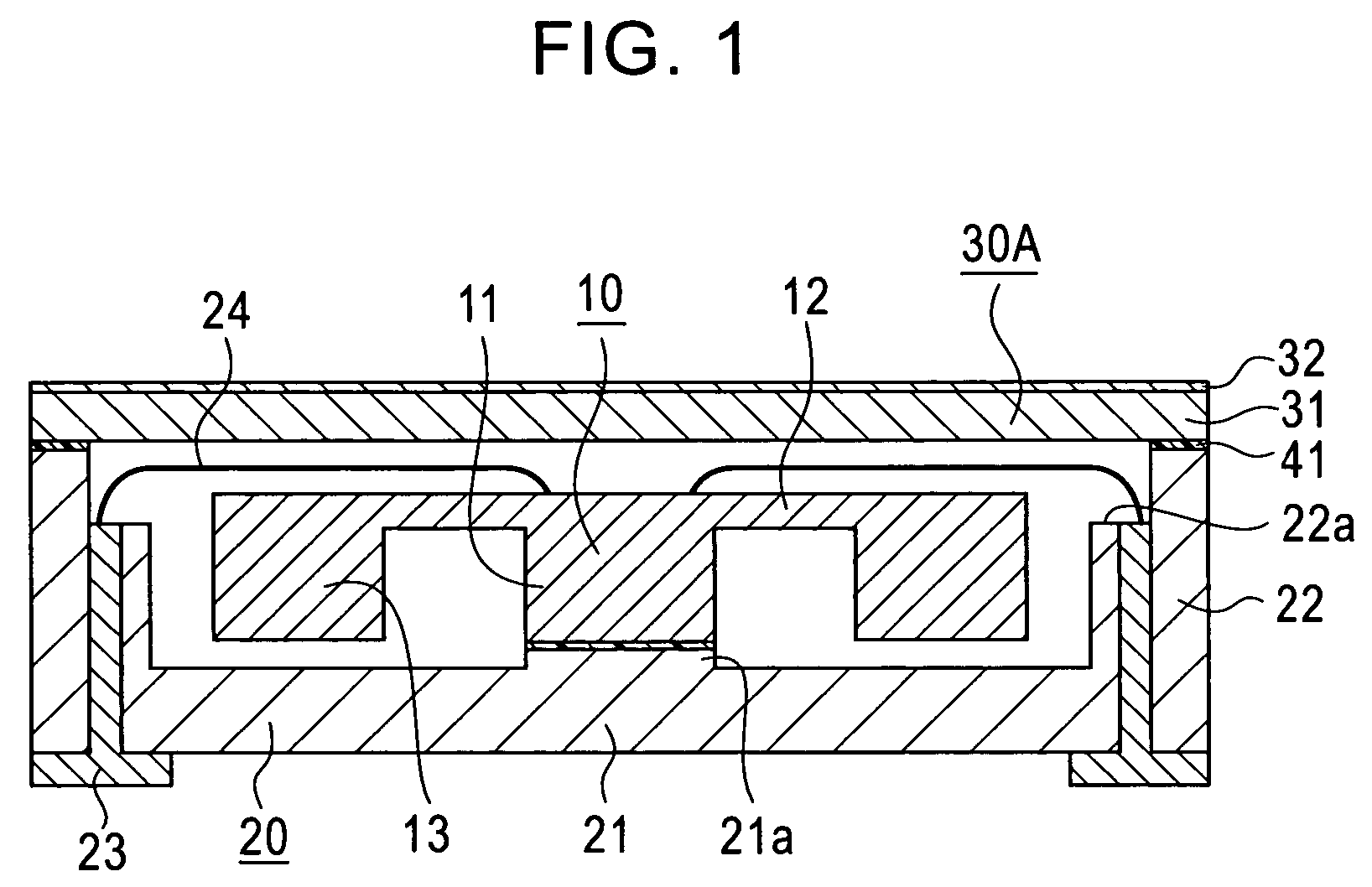
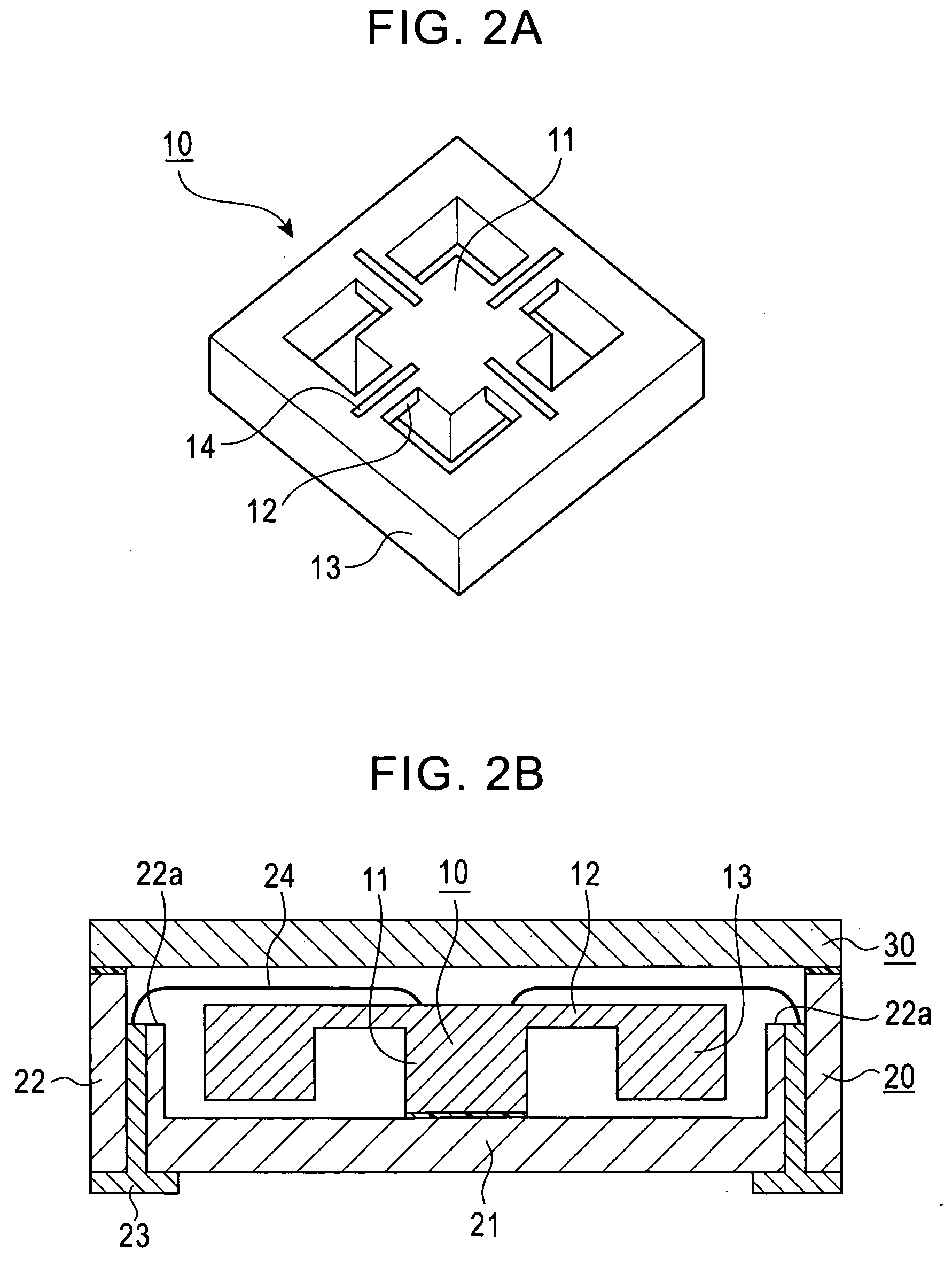
[0024] In FIG. 1, the same reference numerals are used for elements similar to those shown in FIGS. 2A and 2B.

[0025] As shown in FIG. 1, an acceleration sensor includes a sensor body 10 and a ceramic container 20 having the sensor body 10 received therein, which are similar to the sensor body 10 and the ceramic container 20 shown in FIGS. 2A and 2B. The acceleration sensor further includes a lid 30A for sealing a top part of the ceramic container 20, which is different from the lid 30 shown in FIGS. 2A and 2B.

[0026] Specifically, as shown in FIG. 2A, the sensor body 10, for example, includes a fixing part 11 for fixing the sensor body to the package, a weight part 13 supported by four beams 12 extending from the fixing part 11 so as to be displaced due to acceleration, and piezo resistance elements 14 respectively placed at the surfaces of the beams 12. The fixing part 11, the beams 12, and the weight part 13 are integrally shaped and made of silicon.

[0027] The ceramic container ...

second embodiment

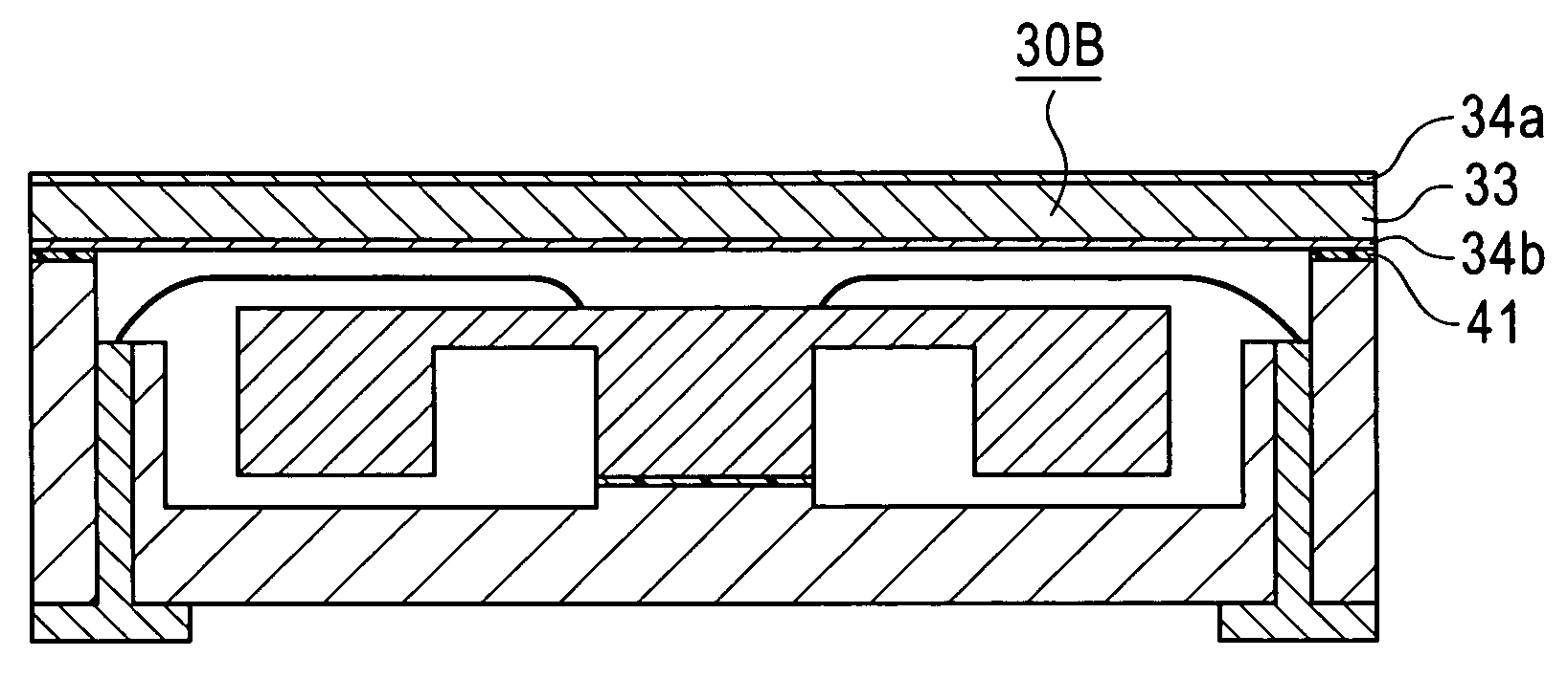
[0037]FIG. 3 is a sectional view showing an acceleration sensor according to a second embodiment of the present invention. In FIG. 3, the same reference numerals are used for elements similar to those used in FIG. 1.

[0038] The acceleration sensor includes a sensor body 10 and a ceramic container 20 having the sensor body 10 received therein, which are similar to the sensor body 10 and the ceramic container 20 shown in FIG. 1. The acceleration sensor further includes a lid 30B for sealing a top part of the ceramic container 20, which is different from the lid 30A shown in FIG. 1.

[0039] The lid 30B is formed by applying copper coating layers 34a and 34b each having a thickness of approximately 10 μm on opposite surfaces of a stainless steel 33 having a thickness of approximately 100 μm, respectively, and then by black-finishing the copper coating layers 34a and 34b by means of oxidization. The lid 30B is fixed to the upper end of the sidewall part 22 of the ceramic container 20 by m...

third embodiment

[0046]FIG. 4 is a sectional view showing an acceleration sensor according to a third embodiment of the present invention. In FIG. 4, the same reference numerals are used for elements similar to those used in FIG. 1.

[0047] The acceleration sensor includes a sensor body 10 and a ceramic container 20 having the sensor body 10 received therein, which are similar to the sensor body 10 and the ceramic container 20 shown in FIG. 1. The acceleration sensor further includes a lid 30C for sealing a top part of the ceramic container 20, which is different from the lid 30A shown in FIG. 1.

[0048] The lid 30C is made of a heat-resistant polyimide tape 35 having a thickness of approximately 100 μm. The lid 30C is fixed to the upper end of the sidewall part 22 of the ceramic container 20 by means of thermosetting resin 41 having a thickness of approximately 20 to 30 μm, in a similar manner as the first embodiment of the present invention. Other construction and operation of the lid 30C are simila...


PUM


Abstract

A lid for sealing a ceramic container receiving a semiconductor device such as an acceleration sensor is provided. The lid has an electrodeposition coating layer having a thickness of approximately 10 μm, which is formed by plating the outer surface of the 42 alloy plate having a thickness of approximately 100 μm with chrome and by forming a black color compound at the chrome plating layer. The lid is fixed to the upper end of a sidewall part of the ceramic container by means of a thermosetting resin. The thickness of the thermosetting resin after thermosetting is adjusted to be approximately 20 to 30 μm. The conventional ceramic lid needs 200 μm or more in thickness in view of strength, and has difficulty in laser processing. The lid of the present invention allows decreasing the thickness by half, and facilitating the imprint by laser.

Description

BACKGROUND OF THE INVENTION [0001] 1. Field of the Invention [0002] The present invention relates to a package for a semiconductor device, and more particularly to the structure of a lid of a package for an acceleration sensor formed by a semiconductor. [0003] 2. Description of the Related Art [0004]FIGS. 2A and 2B are views showing the structure of a conventional acceleration sensor. Specifically, FIG. 2A is a perspective view of a sensor body, and FIG. 2B is a sectional view of a package having the sensor body incorporated therein. [0005] As shown in FIG. 2A, the sensor body 10 includes a fixing part 11 for fixing the sensor body to the package, a weight part 13 supported by four beams 12 extending from the fixing part 11 such that the weight part 13 is displaced due to acceleration, and piezo resistance elements 14 respectively placed at surfaces of the beams 12. The fixing part 11, the beams 12, and the weight part 13 are integrally shaped and made of silicon. [0006] As shown in...

Claims


Application Information

Patent Timeline
IPC IPC(8): H01L23/02G01P15/08
CPCG01P1/023G01P15/123G01P15/18H01L2224/73265H01L2924/01078H01L2924/3025H01L2224/32225H01L2224/48091H01L2924/00014G01P2015/084H01L23/00H01L23/02
Inventor INO, YOSHIHIKO
Owner LAPIS SEMICON CO LTD
Why Eureka
Try Eureka