Module

Inactive Publication Date: 2006-06-22
LONGITUDE LICENSING LTD
View PDF14 Cites 13 Cited by
  • Summary
  • Abstract
  • Description
  • Claims
  • Application Information

AI Technical Summary

Benefits of technology

[0020] In Technique 2, reduction in propagation noise and suppression in surface resonance are effectively conducted by providing individual Vref power source planes to respective memories.
[0021] In Technique 3, propagation noise can be minimized by selecting a wire or a chip part so as to lower propagation impedance. When a chip resistor is used as the chip part, further noise reduction is achieved by inserting a resistor with a resistant value equal to or more than a predetermined resistant value. This is based upon such a method that a Vref feeding ne

Problems solved by technology

In the above-described technique, however, problems (a) that noise generated by a memory itself can not be reduced sufficiently and (b) that propagation noise from another memory on a module can not be reduced sufficiently occur.
The method is effective against the problem (a), but it is not so effective against the problem (b) because a whole Vref feeding network has low impedance over a wide frequency region eve

Method used


Image

  • Module
  • Module
  • Module

Examples


fourth embodiment

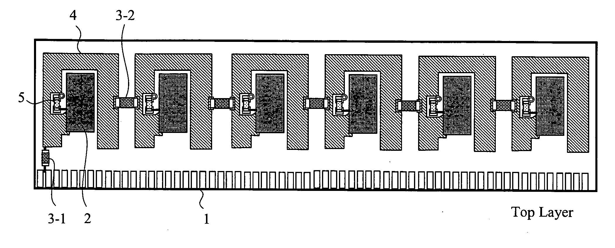
[0094] One example of a memory module according to a fourth embodiment will be explained with reference to FIG. 14.

[0095] The fourth embodiment is an improved one of conventional wire feeding system, where one layer of inner layers is prepared for Vref wiring so that propagation noise is reduced as much as possible.

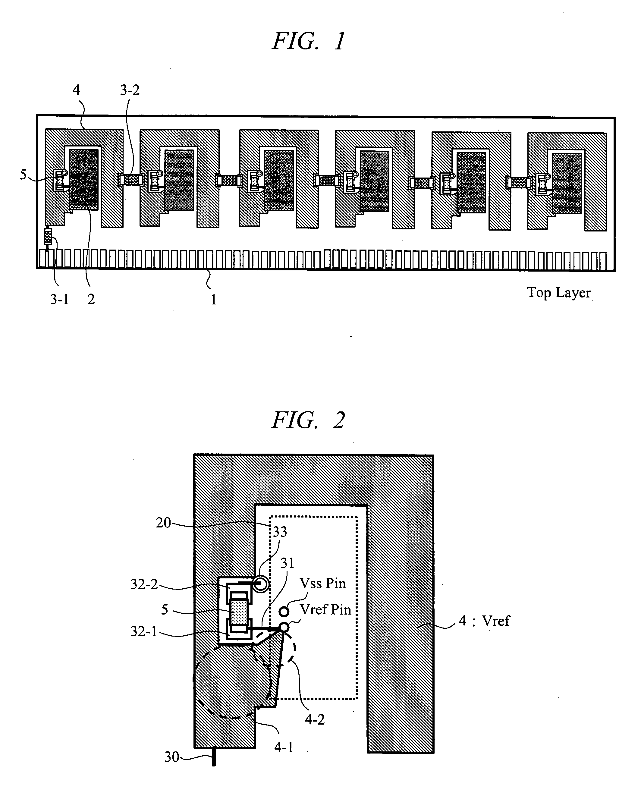
[0096] A wiring method will be explained. A Vref wire from a connector portion is connected to a high impedance chip part 3-1 of an LPF shown in FIG. 14, and after passing through the LPF, it is connected to an inner layer at a Via 34-1. The Vref wire is connected on a Vref layer which is the inner layer from the Via 34-2 to a Vref plane 4-1 prepared just below a mounting position of a first memory by a wire 7-1. The Vref plane 4-1 is connected to a Vref line of a memory through a Via 34-5 connected to a portion of the memory positioned near a Vref pin at a low impedance. A decoupling capacitor 5-1 for Vref is mounted on a TOP layer, and it is connected to the Vref pin ...

fifth embodiment

[0099] The first to fourth embodiments adopt the low noise wiring system in the system where a Vref voltage is supplied from a motherboard. Fifth to eighth embodiments are for realizing a wiring system utilized when Vref is generated inside a module. Basically, the fifth to eighth embodiments have a constitution that the thought (Vref is supplied externally) in the first to fourth embodiments is replaced with Vref internal generation. Here, the Vref internal generation means that, since Vref generally has a voltage value of ½ of a power source voltage Vdd of a memory, it is generated by performing Thevenin's termination on Vdd and Vss in the module. Here, the Thevenin's termination means connecting of Vref wire (plane) to Vdd and Vss respectively using two resistors having the same resistance.

[0100] One example of a memory module according to the fifth embodiment will be explained with reference to FIG. 15.

[0101] The fifth embodiment has a constitution that the first embodiment is...

sixth embodiment

[0102] One example of a memory module according to the sixth embodiment will be explained with reference to FIG. 16.

[0103] The sixth embodiment has a constitution that the second embodiment is modified for Vref internal generation. The sixth embodiment is different from the second embodiment in that there is not any wire from a motherboard (therefore, there is not a Vref wire of the inner layer) and two chip resistors for Vref generation (10-1, 10-2) are mounted on the Vref plane 4-2 in the former.


PUM


Abstract

In a memory module, a plurality of memories are mounted on a module base plate, impedance between Vref and Vss near each memory is coupled to Vss by a decoupling capacitor and a Vref plane to achieve low impedance configuration in a wide frequency range, Vref planes are individually provided for the respective memories, and the Vref planes are connected to each other by using a high impedance wire, or a high impedance chip part. Accordingly, a wiring technique for a module which allows effective reduction of self noise and propagation noise can be provided.

Description

CROSS-REFERENCE TO RELATED APPLICATION [0001] The present application claims priority from Japanese patent application No. JP 2004-365004 filed on Dec. 16, 2004, the content of which is hereby incorporated by reference into this application. BACKGROUND OF THE INVENTION [0002] The present invention relates to a voltage (reference voltage: Vref) that is referred to when a semiconductor device (a memory or the like) used in an information processing device determines a logical value (0 or 1, or the like) in a wiring technique in a module, and in particular to a technique effectively applied in a wiring system for distributing the reference voltage at a low noise level. [0003] For example, semiconductor devices used in an information or data processing device include a device (for example, a DRAM: Dynamic Random Access Memory or the like) which is externally supplied with a reference voltage (Vref) to determine a logical value based upon the voltage. That is, in a binary logic, an input...

Claims


Application Information

Patent Timeline
IPC IPC(8): H05K7/08
CPCH01L23/50H01L23/66H01L24/49H01L25/0657H01L2224/32145H01L2224/48091H01L2224/48145H01L2224/48195H01L2224/48472H01L2224/49H01L2225/0651H01L2924/01003H01L2924/01004H01L2924/01005H01L2924/01013H01L2924/01074H01L2924/01082H01L2924/15311H01L2924/19041H01L2924/19042H01L2924/19043H01L2924/19105H01L2924/30105H01L2924/30107H01L2924/3011H05K1/0227H05K1/023H05K1/0231H05K1/0233H05K1/025H05K1/181H05K2201/093H05K2201/09663H05K2201/10022H05K2201/1003H05K2201/10159H05K2201/10522H05K2201/10545H01L2924/00014H01L24/48H01L2924/01006H01L2924/01019H01L2924/01033H01L2924/00H01L2224/45099H01L2224/05599H01L2924/00012
Inventor UEMATSU, YUTAKAOSAKA, HIDEKINISHIO, YOJIFUNABA, SEIJI
Owner LONGITUDE LICENSING LTD
Why Eureka
Try Eureka