

Non-volatile memory and method for fabricating the same
- Summary
- Abstract
- Description
- Claims
- Application Information
AI Technical Summary
Benefits of technology
Problems solved by technology
Method used
Image

Examples
Embodiment Construction
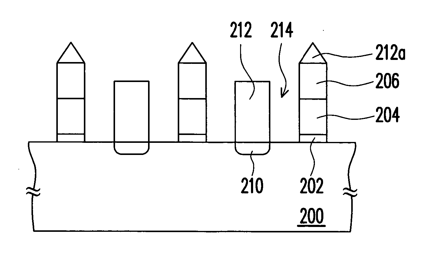
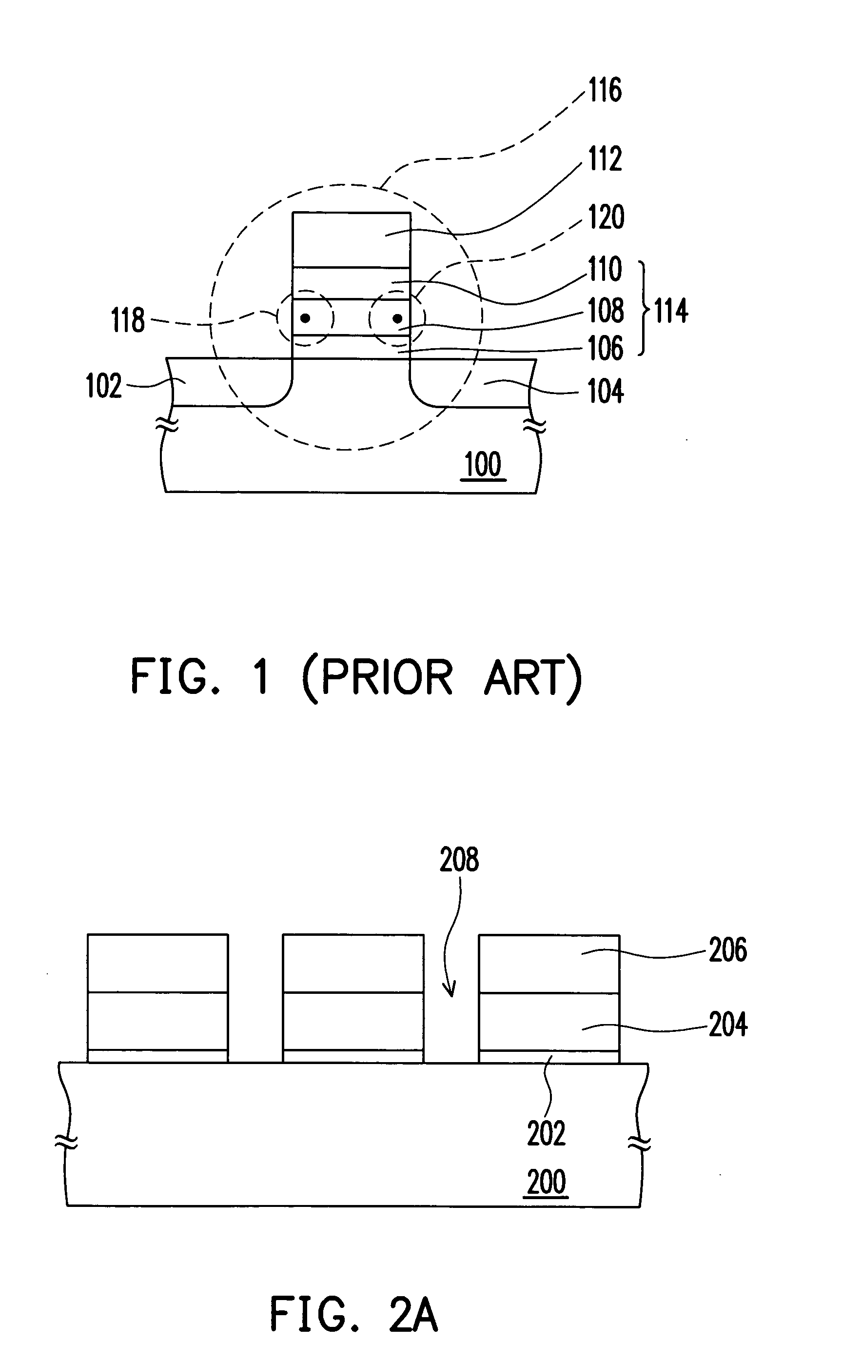
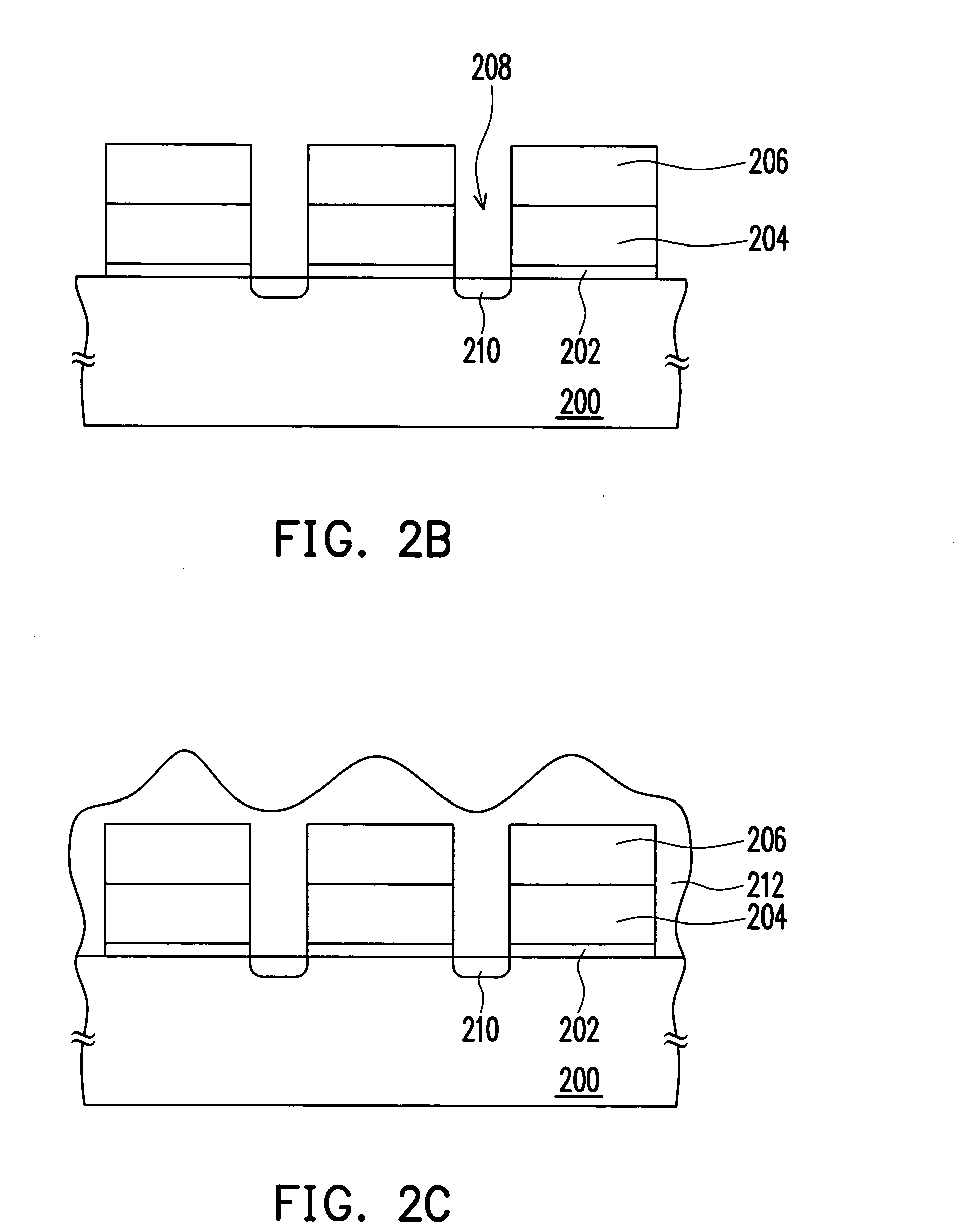
[0032] FIGS. 2A˜2I schematically show cross-sectional views of a flow chart illustrating a method for fabricating a non-volatile memory according to an embodiment of the present invention.
[0033] Referring to FIG. 2A, a substrate 200 is provided, which is, for example, a silicon substrate. Then, a dielectric layer 202 is formed on the substrate 200, wherein the dielectric layer 202 can be made of silicon oxide using a thermal oxidation process, and the dielectric layer 202 is used as a gate oxide layer.
[0034] Then, a conductive layer 204 is formed on the dielectric layer 202, and a mask layer 206 is formed on the conductive layer 204. Wherein, the mask layer 206 can be made of nitride using, for example, a chemical vapor deposition (CVD) process.
[0035] Then, a plurality of openings 208, which expose the substrate 200, are formed by pattering the mask layer 206, the conductive layer 204, and the dielectric layer 202. Wherein, the method for forming the openings 208 exposing the sub...
PUM
 Abstract
Description
Claims
Application Information