Mild methods for generating patterned silicon surfaces
a technology of patterned silicon and surface, applied in the direction of coatings, bulk negative resistance effect devices, material nanotechnology, etc., can solve the problems of destroying or altering the properties of complex biological molecules, lacking silicon integration techniques,
- Summary
- Abstract
- Description
- Claims
- Application Information
AI Technical Summary
Benefits of technology
Problems solved by technology
Method used
Image
Examples
example 1
Materials and Methods
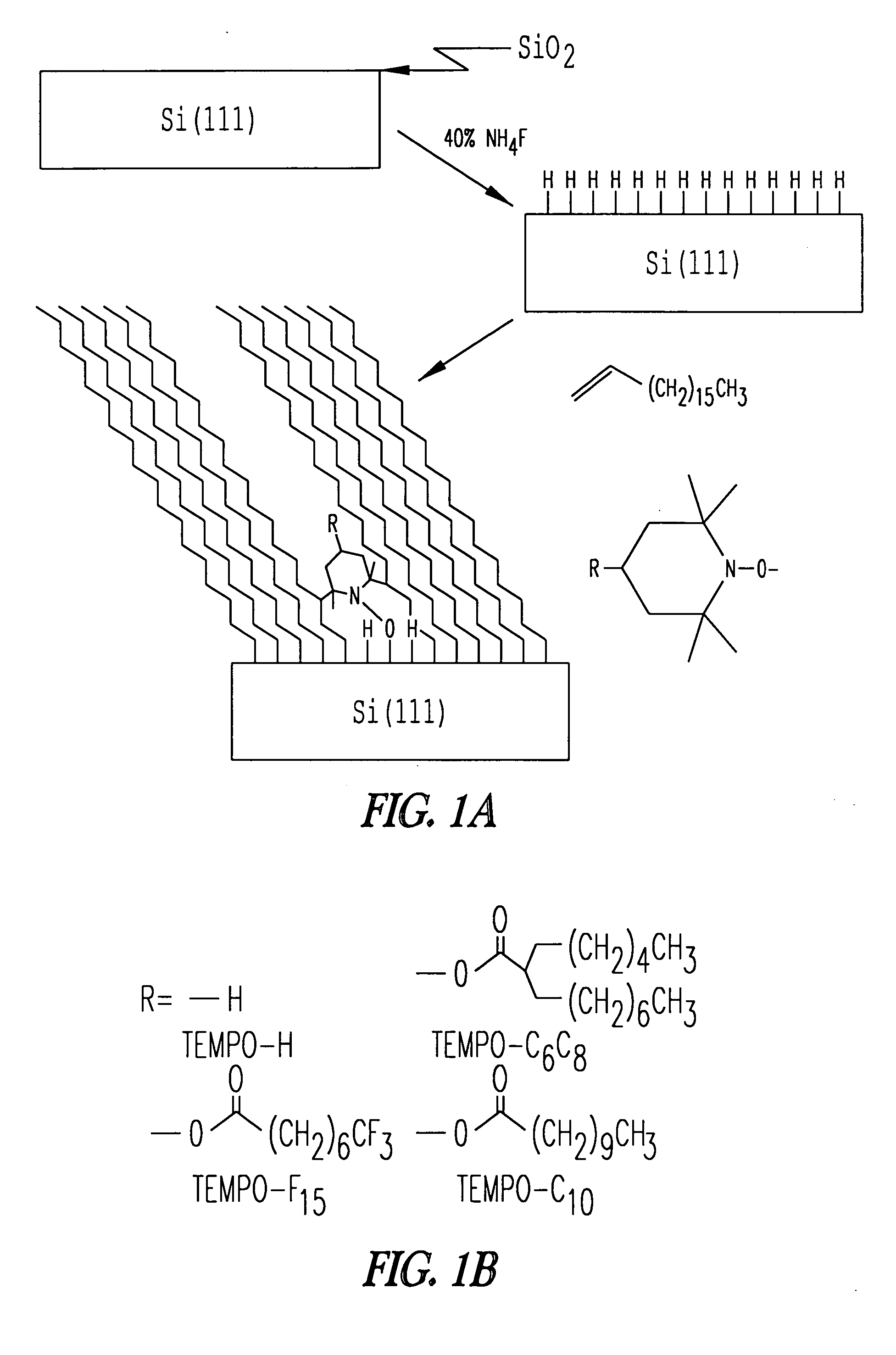
[0068] This Example describes experiments performed to ascertain whether 2,2,6,6-tetramethyl-1-piperidinyloxy (TEMPO) could promote self-assembly of a monolayer on a Si(111)-H surface in the presence of an olefin. Si(111)-H was chosen because it can be easily formed in high yield, it is atomically flat, and it has few dangling reactive moieties.5 TEMPO is a stable free radical that is not reactive with most functional groups at room temperature. As illustrated below, monolayer assembly on Si(111)-H surfaces can be performed at room temperature using TEMPO and related sterically hindered free radical sources.
Materials
[0069] Distilled water, 1-octadecene (90%), hexane, 2,2,6,6-tetramethyl-1-piperidinyloxy (TEMPO, 98%), 4-hydroxy-2,2,6,6-tetramethylpiperidinyloxy, pentadecafluorooctanoyl chloride (97%), undecanoic acid (99%), oxalyl chloride (98%), Al2O3 (basic, Brockman activity 1), 2-hexyldecanoic acid, 4-dimethylamino)pyridine (99%), and 48% hydrofluoric aci...
example 2
Monolayer Assembly on Si(111)-H Surfaces Proceeds Under Mild Conditions in the Presence of TEMPO
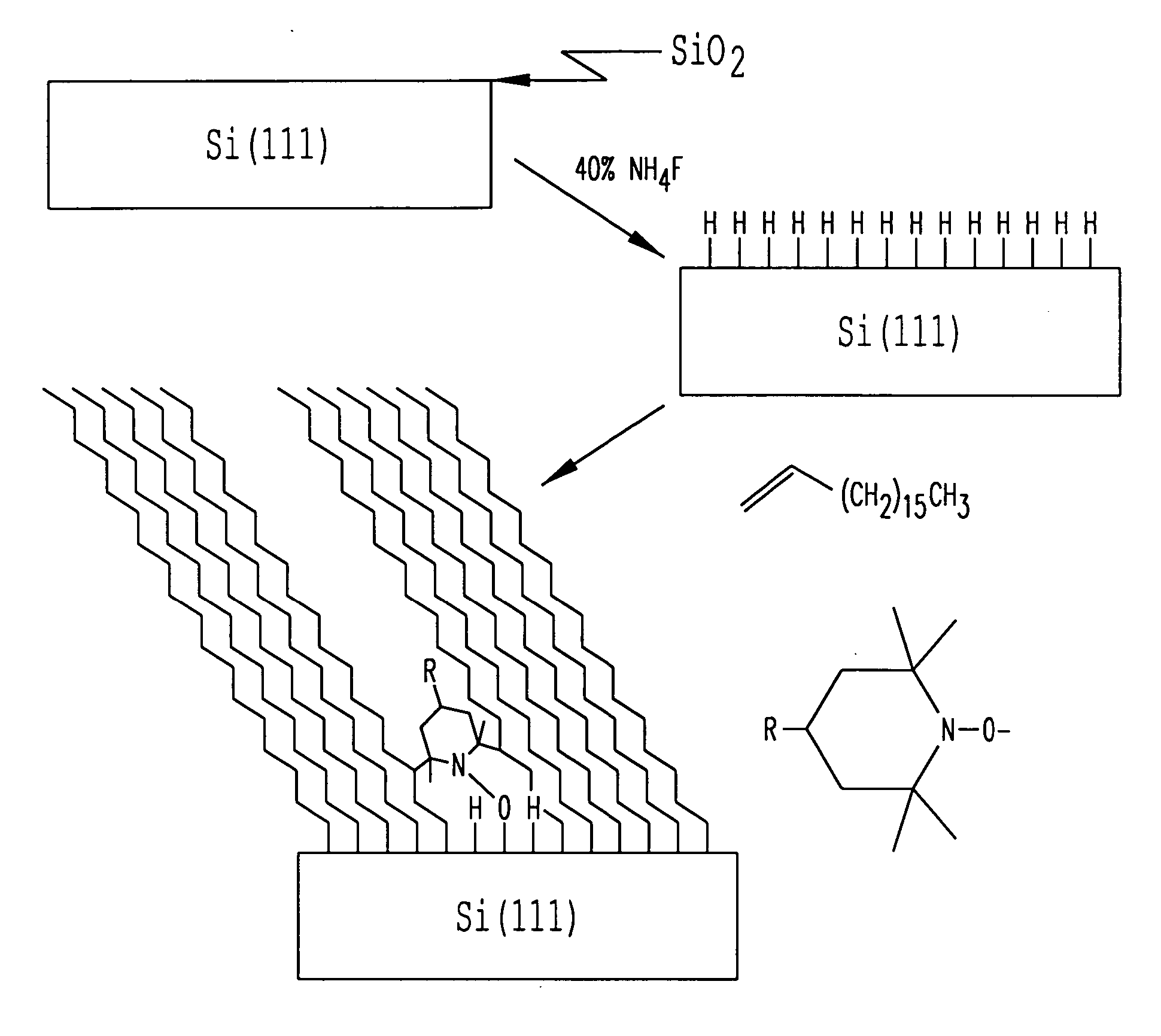
[0084] The reaction of TEMPO and 1-octadecene with Si(111)-H was performed at room temperature as illustrated schematically in FIG. 1, and as described in detail in Example 1. Briefly, silicon wafers were cleaned in organic solvents and the native silicon dioxide layer was removed with 5:1 40% NH4F / 48% HF at. A thin layer of silicon dioxide on the wafer was generated by placing the wafer in 1:3 30% H2O2 / concentrated sulfuric acid at 90° C. for 1 hour. Si(111)-H was formed on the wafer surface by immersion of the wafer in 40% NH4F under an atmosphere of argon using procedures generally outlined in Wade et al. APPL. PHYS. LETT. 71: 1679-81 (1997) and Higashi et al. APPL. PHYS. LETT 56: 656-658 (1990). The silicon wafer was then placed in a schlenk flask of TEMPO and 1-octadecene in a glove box under N2. The formation of the monolayer was initially monitored by following the advancing conta...
example 3
Cross Metathesis on Olefin-Terminated Monolayers on Si(111) Using Grubbs' Catalyst
[0091] This Example describes the functionalization and patterning of olefin-terminated monolayers on Si(111) through cross metathesis. A simple, one-step synthesis of a diolefin —CH2═CH(CH2)9O(CH2)9CH═CH2—was developed from commercially available starting materials. Mixed partially olefin-terminated monolayers of this novel diolefin and 1-octadecene on hydrogen-terminated Si(111) were obtained. The olefins are raised above the rest of the monolayer and thus sterically accessible for further functionalization. Olefin-terminated monolayers were reacted with the Grubbs' first generation catalyst and olefins in solution that were terminated with fluorines, carboxylic acids, alcohols, aldehydes, and alkyl bromides. Characterization of these monolayers using x-ray photoelectron spectroscopy and horizontal attenuated total reflection infrared spectroscopy demonstrated that olefins on the surface had reacted...
PUM
| Property | Measurement | Unit |
|---|---|---|
| contact angle | aaaaa | aaaaa |
| contact angle | aaaaa | aaaaa |
| contact angle | aaaaa | aaaaa |
Abstract
Description
Claims
Application Information


