Method of manufacturing wiring board

Active Publication Date: 2006-06-29
SHINKO ELECTRIC IND CO LTD
View PDF7 Cites 12 Cited by
  • Summary
  • Abstract
  • Description
  • Claims
  • Application Information

AI Technical Summary

Benefits of technology

[0020] In light of the problems as described above, in a particular embodiment of the present invention is provided a method of manufacturing a wiring board that makes it possible to make the reliability of the connection of a decoupling capacitor mounted on the wiring board superior.
[0022] The wiring board in an embodiment of the invention makes it possible to make the reliability of the connection of the decoupling capacitor superior.

Problems solved by technology

However, for installing a decoupling capacitor in a wiring board on which a semiconductor chip is mounted, a problem could arise with the reliability of the wiring structure to which the decoupling capacitor and the semiconductor chip are connected.
However, as the via wiring and pattern wiring connected to the via wiring are minituarized, problems could arise with the registration tolerance (the alignment tolerance) of the via wiring, or with the reliability of the connection between the via wiring and electrode layers of the decoupling capacitor, or with the reliability of the connection between the via wiring and the pattern wiring, possibly making it difficult to make a low-impedance structure which is superior in the reliability of the connection.

Method used


Image

  • Method of manufacturing wiring board
  • Method of manufacturing wiring board
  • Method of manufacturing wiring board

Examples


embodiment 1

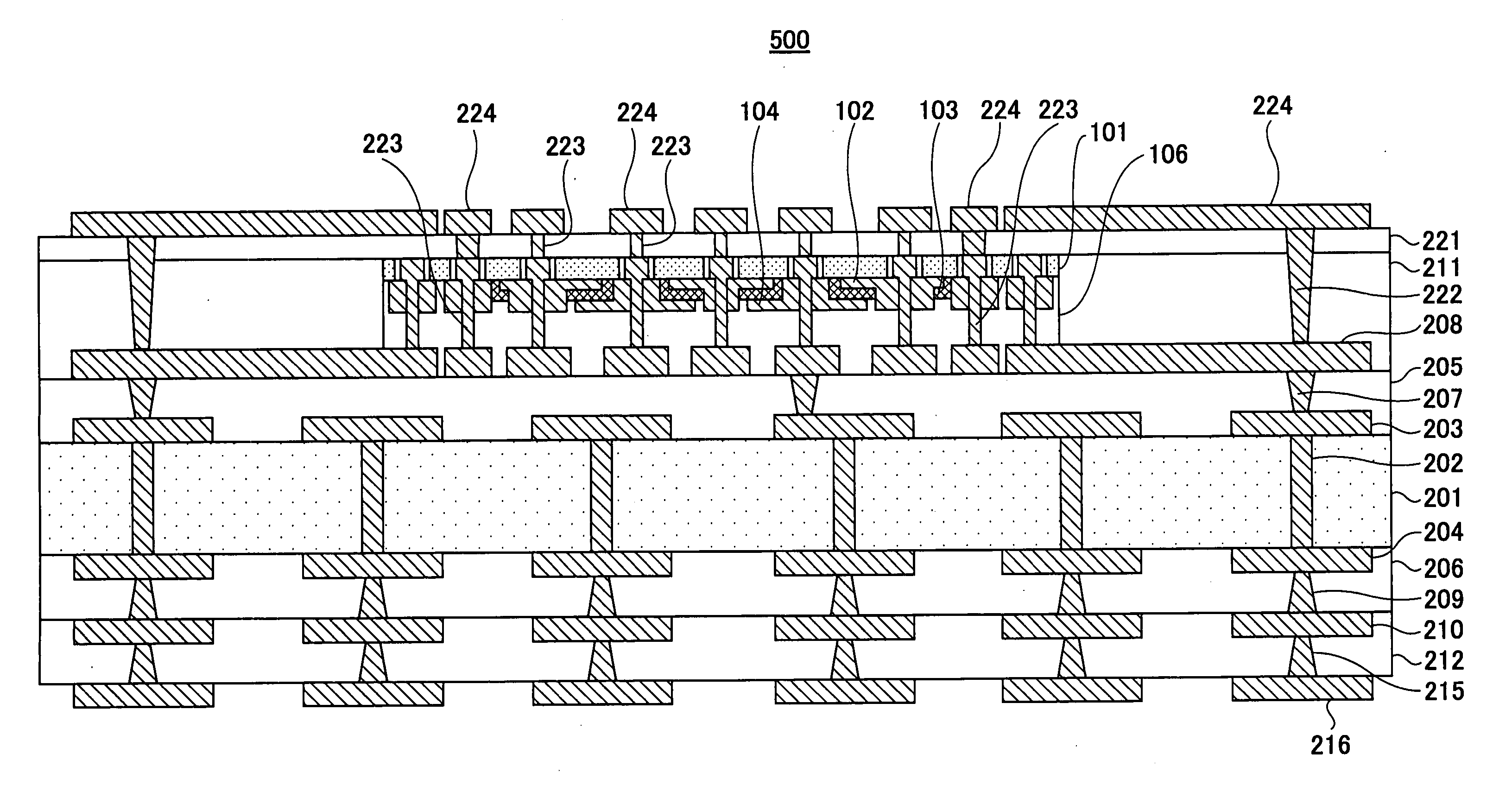
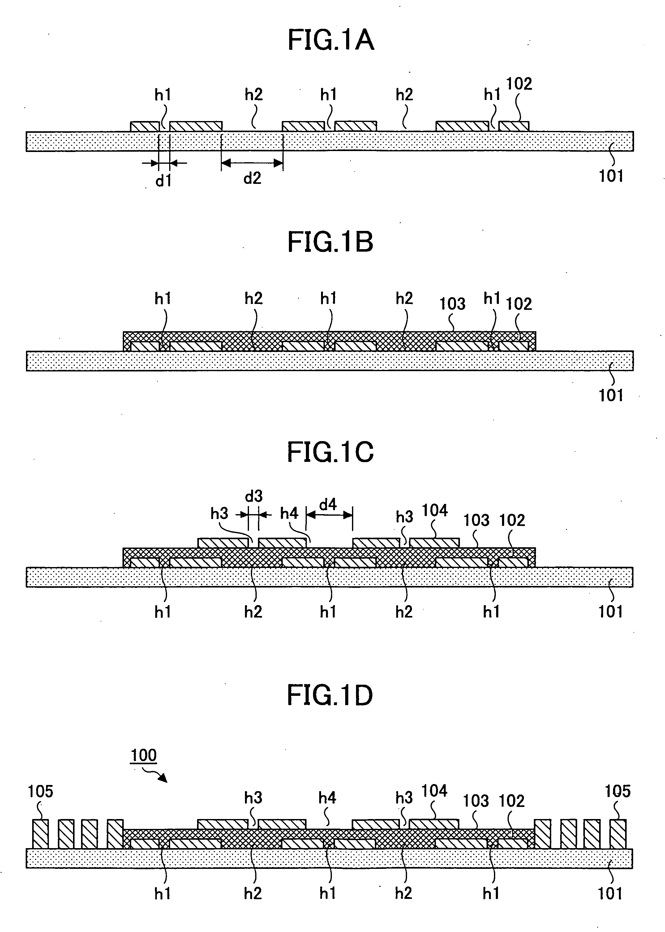
[0048] In the present embodiment, a method is described of manufacturing a wiring board to which a semiconductor chip is connected, in which wiring board is installed a decoupling capacitor (below described as the capacitor) for stabilizing the power supply voltage of the semiconductor chip.

[0049] In the method of manufacturing the wiring board according to the present embodiment, it is possible to simplify the wiring structure to which the capacitor and the semiconductor chip are connected. In the wiring board manufactured using the present embodiment, it is possible to reduce the impedance pertaining to the connection of the semiconductor chip and the capacitor so as to reduce noise of the power supply line and stabilize the power supply voltage.

[0050] In this way, with the wiring board according to the present embodiment, the capacitor and the semiconductor chip are connected using via wiring which pierces the capacitor in order to simplify the structure to which the capacitor ...

embodiment 2

[0104] Moreover, when the core substrate 101 is formed with a non-insulator material (for example, silicon, etc.), a wiring board may be formed using a method as shown below. Even in this case, the same advantage as is shown for the embodiment 1 is provided.

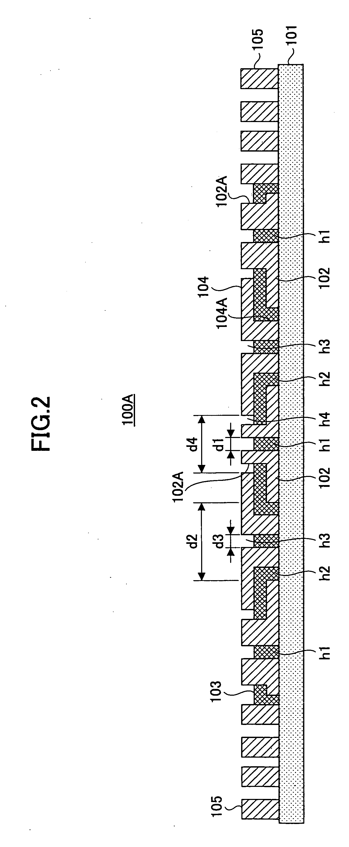
[0105] For the present embodiment, the structure of the capacitor 100A is the same as is illustrated in FIG. 2.

[0106] For the present embodiment, the wiring board is formed following such processes as shown in FIGS. 9A through 9F below after forming the capacitor 100A.

[0107] First, in the process as illustrated in FIG. 9A, an insulating layer 110 consisting of a resin material such as epoxy is formed on the capacitor 100A as illustrated in FIG. 2 by laminating or applying, and via holes BH3 which pierce the core substrate 101 so as to reach the insulating layer 110 are formed with a laser from the side of the core substrate 101. Here, it is preferable that the laser processing diameter be larger than the diameter d1 of the thr...


PUM


Abstract

A method of manufacturing a wiring board is disclosed. The wiring board has: a capacitor, having multiple electrode layers which oppose each other with a dielectric layer in between, that is connected to a semiconductor chip; one or more via wirings which pierce the electrode layers and which are connected to the semiconductor chip, and pattern wirings connected to the via wirings. The method includes: forming the electrode layers, each having one or more through holes which the via wirings pierce, and the dielectric layer, and forming the capacitor; installing the capacitor such that the capacitor opposes the pattern wirings over an insulating layer; forming one or more via holes which reach the pattern wirings from the through holes; and forming the via wiring in the via hole.

Description

BACKGROUND OF THE INVENTION [0001] 1. Field of the Invention [0002] The present invention generally relates to a wiring board, and particularly relates to a method of manufacturing a wiring board having a decoupling capacitor which is connected to a semiconductor chip. [0003] 2. Description of the Related Art [0004] In recent years, with a semiconductor device such as a semiconductor chip becoming smaller and thinner, there has been a need to make a decoupling capacitor (which may also be called a bypass capacitor) smaller for suppressing changes in the power supply voltage of the semiconductor chip so as to stabilize its operation, and to use thin-film technologies for the decoupling capacitor. [0005] Moreover, as the operating frequency of the semiconductor chip is expected to become higher in order to further increase the operating speed of the semiconductor chip in the future, the decoupling capacitor is preferably installed in the vicinity of the semiconductor chip in order to ...

Claims


Application Information

Patent Timeline
IPC IPC(8): H01L21/4763
CPCH01L23/49822H01L23/50H01L2924/3011H05K1/113H05K1/162H05K3/20H05K3/4644H05K2201/096H05K2201/09763H05K2201/10674H05K2203/016H05K2203/0733H01L2924/0002H01L2924/00
Inventor OI, KIYOSHISHIMIZU, NORIYOSHIYAMASAKI, TOMOO
Owner SHINKO ELECTRIC IND CO LTD
Why Eureka
Try Eureka