Light emitting device and process for fabricating the same
a technology of light emitting device and process, which is applied in the direction of semiconductor devices, basic electric elements, electrical apparatus, etc., can solve the problem of limit on the positional relation of conductivity, and achieve the effect of lowering reflectivity, reducing emission intensity, and desirable reflectivity
- Summary
- Abstract
- Description
- Claims
- Application Information
AI Technical Summary
Benefits of technology
Problems solved by technology
Method used
Image

Examples
Embodiment Construction
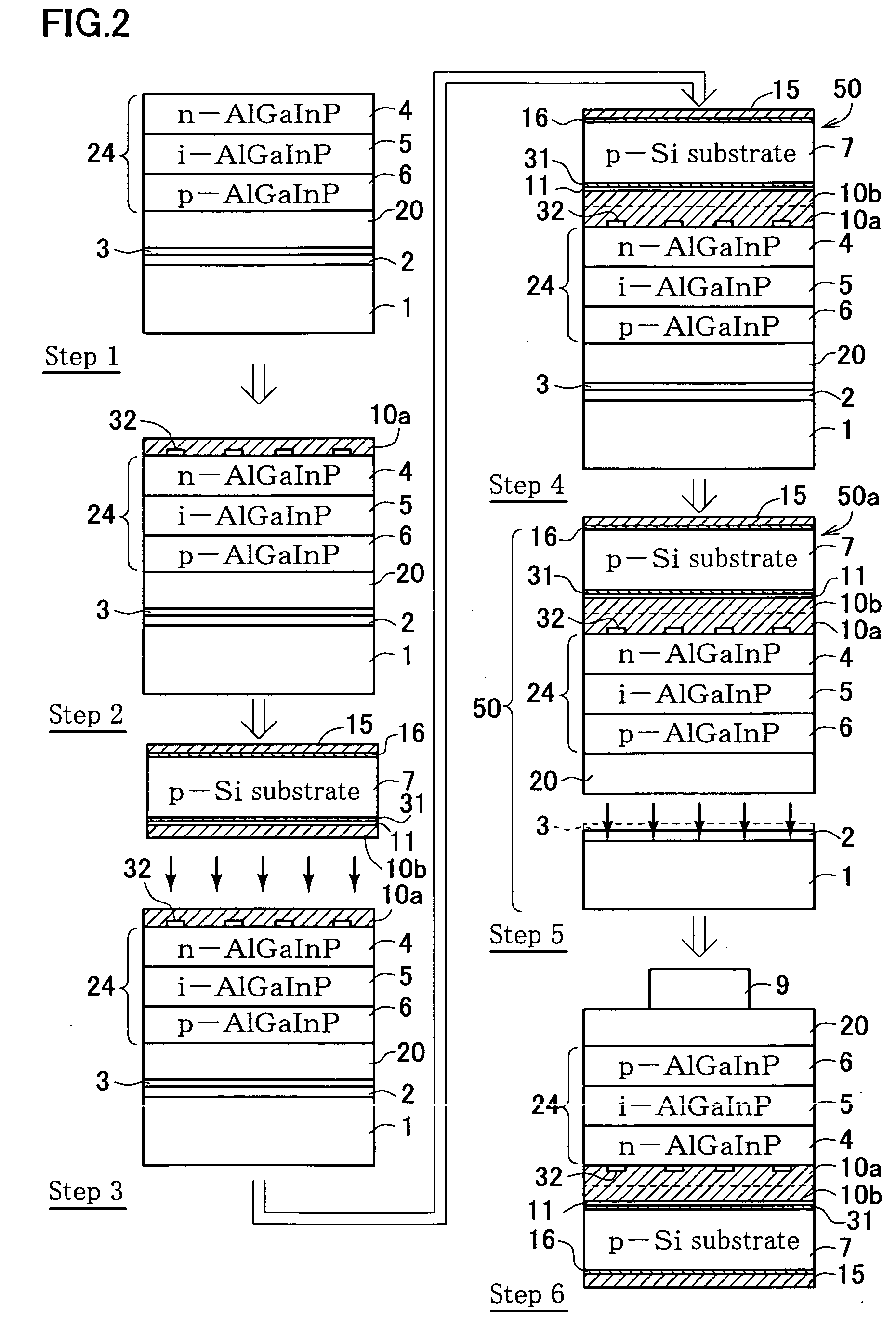
[0034] The following paragraphs will describe best modes for carrying out this invention, referring to the attached drawings.
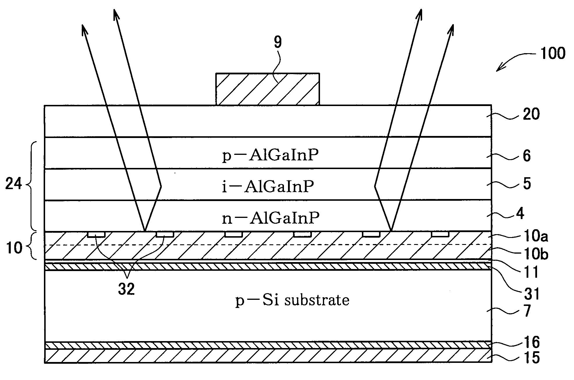
[0035]FIG. 1 is a conceptual drawing showing a light emitting device 100 as one embodiment of the invention. The light emitting device 100 is configured so that a light emitting layer section 24 is bonded, while placing a main metal layer 10 in between, to a first main surface of p-Si substrate 7 composed of a p-type Si (silicon) single crystal which is a electro-conductive substrate serves as the device-substrate.
[0036] The light emitting layer section 24 has a structure in which an active layer 5 composed of non-doped (AlxGa1-x)yIn1-yP (where, 0≦x≦0.55, 0.45≦y≦0.55) is held between a first conductivity type cladding layer, which is a p-type cladding layer 6 composed of p-type (AlzGa1-z)yIn1-yP (where x4 composed of n-type (AlzGa1-z)yIn1-yP (where x100, the p-type AlGaInP cladding layer 6 is disposed on the metal electrode layer 9 side, and the n-type AlGaI...
PUM
 Abstract
Description
Claims
Application Information
 - Generate Ideas
- Intellectual Property
- Life Sciences
- Materials
- Tech Scout
- Unparalleled Data Quality
- Higher Quality Content
- 60% Fewer Hallucinations
Browse by: Latest US Patents, China's latest patents, Technical Efficacy Thesaurus, Application Domain, Technology Topic, Popular Technical Reports.
© 2025 PatSnap. All rights reserved.Legal|Privacy policy|Modern Slavery Act Transparency Statement|Sitemap|About US| Contact US: help@patsnap.com