Semiconductor package

Inactive Publication Date: 2006-07-06
ADVANCED SEMICON ENG INC
View PDF12 Cites 22 Cited by
  • Summary
  • Abstract
  • Description
  • Claims
  • Application Information

AI Technical Summary

Benefits of technology

[0009] A semiconductor package having features of the present invention generally includes a semiconductor device and a passive component mounted and electrically coupled to a substrate. To achieve the above listed and other objects, the passive component is disposed within a cavit

Problems solved by technology

As the speed of electronic packages increase, noise in the DC power and ground lines increasingly becomes a problem.
However, mounting the passive components directly to the substrate, as in many prior art packages, creates several problems.
First, the requirement for the passive compon

Method used


Image

  • Semiconductor package
  • Semiconductor package
  • Semiconductor package

Examples


Example

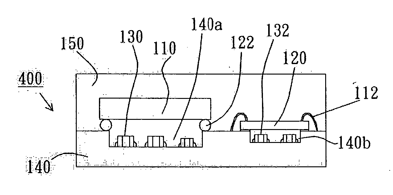
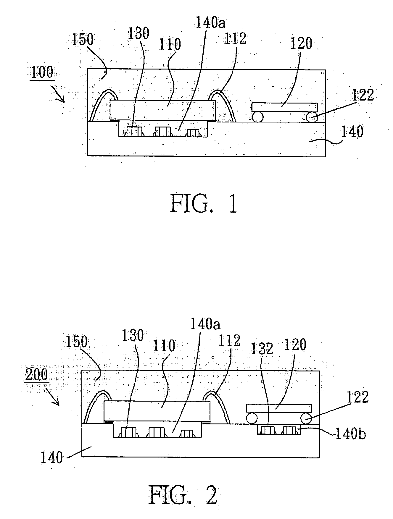
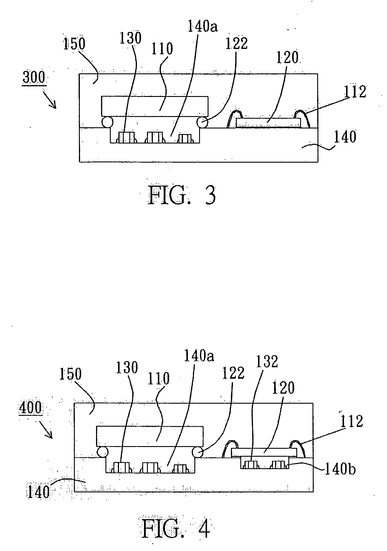
[0023]FIG. 1 shows a semiconductor package 100 according to one embodiment of the present invention. The semiconductor package 100 includes two semiconductor devices 110 and 120, and a plurality of passive components 130 mounted and electrically coupled to a substrate 140. Note that all of the passive components 130 are disposed within a cavity portion 140a formed on an upper surface of the substrate 140 and the semiconductor device 110 is disposed across the cavity portion 140a of the substrate 140 above the passive components 130, thereby significantly reducing overall thickness of the package 100 so as to increase the packaging efficiency.

[0024] The semiconductor device 110 is attached to the substrate 140 by means of an adhesive layer or a double-coated adhesive tape. The adhesive layer may be conductive, e.g., a silver-filled epoxy, or non-conductive. The semiconductor device 110 is connected to the substrate 140 by a plurality of bonding wires 112 which act as electrical inpu...


PUM


Abstract

A semiconductor package includes a semiconductor device and a passive component mounted and electrically coupled to a substrate. The passive component is disposed within a cavity portion formed on an upper surface of the substrate and the semiconductor device is disposed across the cavity portion of the substrate above the passive component.

Description

BACKGROUND OF THE INVENTION [0001] 1. Field of the Invention [0002] The present invention relates to semiconductor packages, and more specifically to semiconductor packages having passive components. [0003] 2. Description of the Related Art [0004] A semiconductor package typically includes a circuitized substrate with one or more active devices attached thereon; packages including only one device are known as Single Chip Modules (SCM), while packages including a plurality of devices are called Multi Chip Modules (MCM). The active device is typically a chip, a small piece of a wafer a commonly made of Silicon, Germanium or Gallium Arsenide. [0005] As the speed of electronic packages increase, noise in the DC power and ground lines increasingly becomes a problem. To reduce this noise, passive components such as decoupling capacitors are often used to reduce power supply noise which occurs due to change in potential difference between the ground voltage and the power-supply voltage sup...

Claims


Application Information

Patent Timeline
IPC IPC(8): H01L23/34H01L23/06H01L23/02
CPCH01L23/13H01L2924/07802H01L24/32H01L25/16H01L2224/16225H01L2224/32014H01L2224/32057H01L2224/32145H01L2224/32225H01L2224/48091H01L2224/48227H01L2224/73265H01L2224/83385H01L2924/01032H01L2924/01047H01L2924/01079H01L2924/15153H01L2924/15165H01L2924/19041H01L2924/19042H01L2924/19043H01L2924/19103H01L2924/19105H01L2924/30107H01L2924/3011H05K1/023H05K1/183H05K2201/09036H05K2201/10515H05K2201/10674H01L23/3121H01L2924/1515H01L2224/16145H01L2924/01033H01L24/48H01L2924/00014H01L2924/00H01L2924/00012H01L24/73H01L2924/181H01L2924/15159H01L2924/00011H01L2224/0401H01L2224/45099H01L2224/45015H01L2924/207
Inventor YANG, JUN YOUNGJOO, YOU OCKJUNG, DONG PIL
Owner ADVANCED SEMICON ENG INC
Why Eureka
Try Eureka