DRAM with high K dielectric storage capacitor and method of making the same

a dielectric storage capacitor and high k dielectric technology, applied in the field of dielectric storage capacitors with high k dielectric storage capacitors and a method of making the same, can solve the problem of slow leakage of capacitor charge, and achieve the effect of minimizing the interfacial contribution to eo

Inactive Publication Date: 2006-07-13
INFINEON TECH AG
View PDF53 Cites 15 Cited by
  • Summary
  • Abstract
  • Description
  • Claims
  • Application Information

AI Technical Summary

Benefits of technology

[0011] Metals, such as titanium, form a solid solution with oxygen and are, therefore, very effective as gettering layers. Furthermore, formation of a conductive silicide layer at the interface would be very useful for creating MIM capacitors. Alternatively, if processing conditions are selected such that a silicate layer forms, the uniformity and higher dielectric constant of such a layer would help to minimize the interfacial contribution to EOT. The segregation of oxygen can be tailored (through temperature, time, and partial pressure control) such that a pure silicide is in contact with the silicon substrate and the silicate/oxide is formed above the silicide layer.
[0012] The high K layer is based on TiO2, which has a dielectric constant in the range of 80. However, TiO2 by itself will not be adequate due to the low band gap (˜3.05 eV) and the negligible conduction band offset to Si (close to 0 eV). Combining TiO2 with higher band gap materials (even tho

Problems solved by technology

In any practical device, charge will slowly leak from the capacitor.
A key challenge is t

Method used


Image

  • DRAM with high K dielectric storage capacitor and method of making the same
  • DRAM with high K dielectric storage capacitor and method of making the same
  • DRAM with high K dielectric storage capacitor and method of making the same

Examples


Embodiment Construction

[0019] The making and using of the presently preferred embodiments are discussed in detail below. It should be appreciated, however, that the present invention provides many applicable inventive concepts that can be embodied in a wide variety of specific contexts. The specific embodiments discussed are merely illustrative of specific ways to make and use the invention, and do not limit the scope of the invention.

[0020] The present invention will be described with respect to preferred embodiments in a specific context, namely a DRAM cell. The invention may also be applied, however, to other devices that include capacitors. For example, any integrated circuit that uses a capacitor can benefit from the teachings of the present invention.

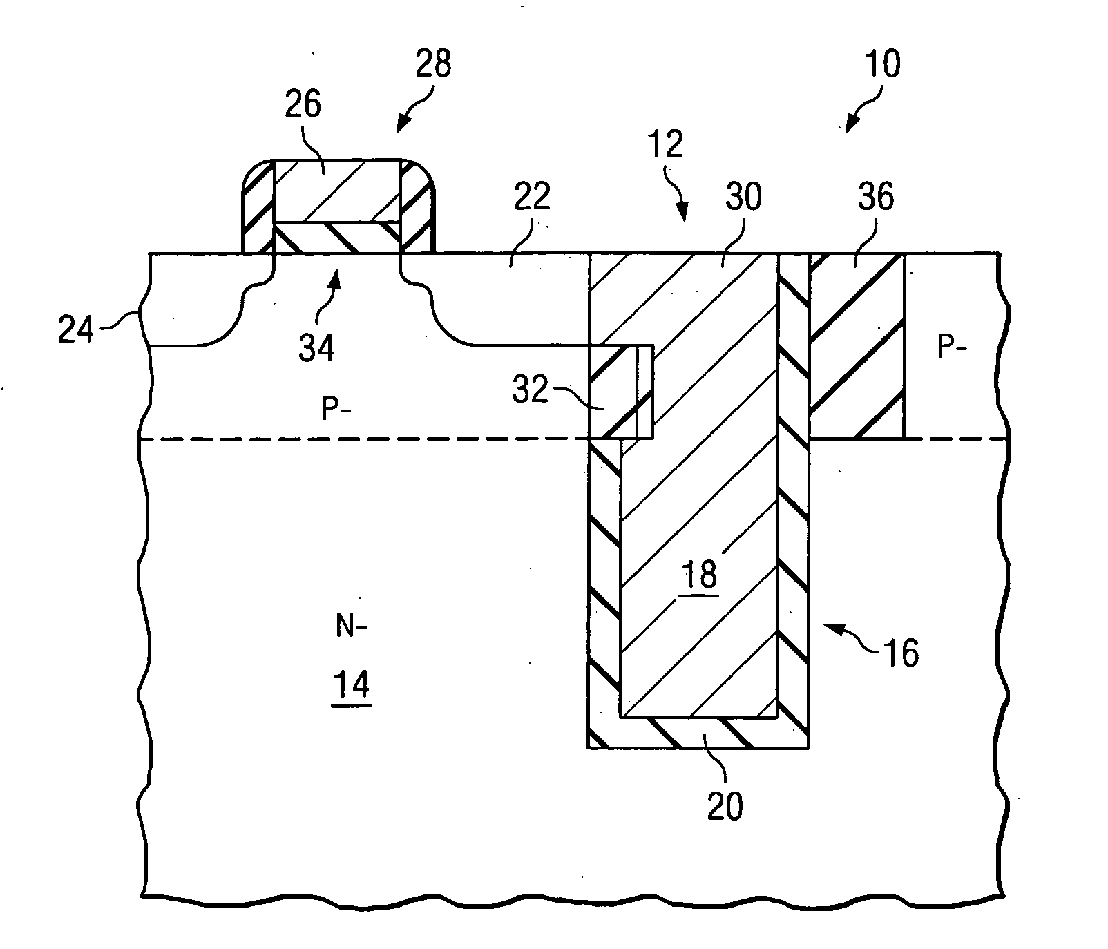
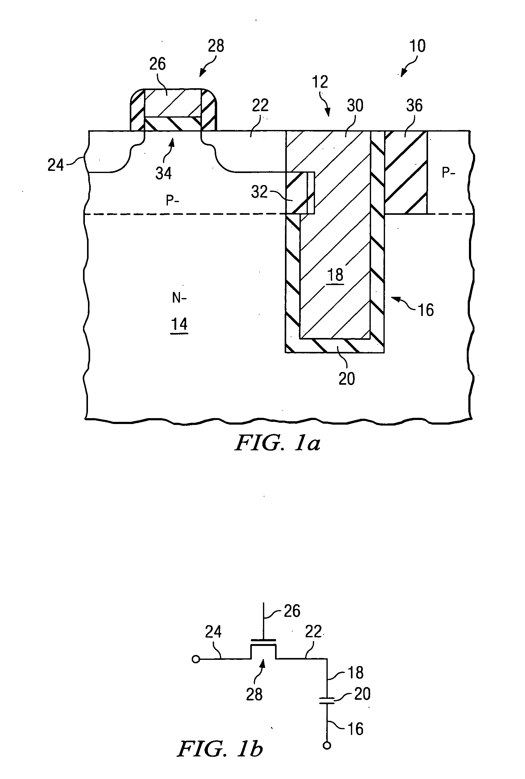
[0021]FIG. 1a shows a first example of a DRAM cell 10 that can utilize concepts of the present invention. FIG. 1b shows a schematic diagram of the cell of FIG. 1a. The embodiment of FIG. 1a includes a trench capacitor 12, which is formed in the semico...


PUM


Abstract

A dynamic random access memory cell that includes a transistor formed in a semiconductor body. A capacitor is coupled to the transistor and includes a first capacitor plate formed from silicon. A metal layer is adjacent to and electrically coupled to the first capacitor plate. A capacitor dielectric layer is adjacent to the metal layer. The capacitor dielectric layer comprises material having a dielectric constant greater than about 5. A second capacitor plate is adjacent to the capacitor dielectric. The capacitor can be either a trench capacitor or a stacked capacitor.

Description

CROSS-REFERENCE TO RELATED APPLICATIONS [0001] This application is related to the following co-pending applications, both of which are incorporated herein by reference: application Ser. No. ______, filed ______, and entitled “High Dielectric Constant Materials” (Attorney Docket 2004P54456) and application Ser. No. ______, filed ______, and entitled “Method to Control Interfacial Properties for Capacitors Using a Metal Layer” (Attorney Docket 2004P54458).TECHNICAL FIELD [0002] The present invention relates generally to semiconductor devices and methods, and more particularly to a DRAM with a high K dielectric storage capacitor and a method of making the same. BACKGROUND [0003] A dynamic random access memory (DRAM) is a memory device that can be used to store information. DRAMs are favored in some applications because they are relatively inexpensive to fabricate in very high densities. Each DRAM cell typically includes two elements, namely a storage capacitor and an access transistor....

Claims


Application Information

Patent Timeline
IPC IPC(8): H01L29/94
CPCH01L27/1087H01L29/945H10B12/0387
Inventor GOVINDARAJAN, SHRINIVAS
Owner INFINEON TECH AG
Why Eureka
Try Eureka