Miniature electro-optic device and corresponding uses thereof

a technology of electro-optic devices and miniature surfaces, applied in the direction of micromechanical switches, gyroscopes/turn-sensitive devices, acceleration measurement using interia forces, etc., can solve the problems of reducing and impeding their advance, so as to improve the accuracy of miniaturisation techniques and reduce wear. , the effect of simple detection of switching tim

Inactive Publication Date: 2006-07-13
BAOLAB MICROSYST
View PDF3 Cites 27 Cited by
  • Summary
  • Abstract
  • Description
  • Claims
  • Application Information

AI Technical Summary

Benefits of technology

[0026] A preferred embodiment is achieved when the first condenser plate is in the second zone. Alternatively the electro-optical device can be designed so that the first condenser plate is in the first zone. In the first case an electro-optical device is obtained which has a lower activation voltage and which is faster. On the other hand, in the second case the electro-optical device is slower, which means that the shocks experienced by the conductive element and the stops are gentler, and energy consumption is lower. In this way, one can choose between one and the other alternative depending on the specific requirements in each case.
[0052] In general, in all sensors cited above one can determine the corresponding magnitude by detecting in each case what is the minimum voltage necessary to switch the electro-optical device, or detect which is the switching time for a fixed applied voltage. In general it is simpler to detect the switching time, since it can be increased very simply using digital technology, while generating variable voltages implies using analogue circuits. However when detecting the voltage which switches the electro-optical device, there is the advantage that the electro-optical device commutates much less frequently, reducing wear and increasing long term reliability and working life.

Problems solved by technology

However miniaturisation techniques require the use of the smallest possible activation voltages and the smallest possible surfaces.
The relays known in the state of the art have several problems impeding their advance in this respect.
A manner of reducing the activation voltage is precisely to increase the relay surface areas, which renders miniaturisation difficult, apart from being conducive to the appearance of deformations reducing the useful life and reliability of the relay.
However this implies problems of sticking, since capillary forces are very high, which thus also reduces the useful working life and reliability of these relays.
The use of high activation voltages also has negative effects such as ionisation of the components, accelerated wearing due to strong mechanical solicitation and the electric noise which the whole relay generates.
Electrostatic relays also have a significant problem as to reliability, due to the phenomenon known as “pull-in”, and which consists in that, once a given threshold has been passed, the contact electrode moves with increasing acceleration against the other free electrode.
Consequently there is a significant wear on the electrodes due to the high electric field which is generated and the shock caused by the acceleration to which the moving electrode has been exposed.
The thermal, magnetic and piezoelectric approaches require special materials and micromachining processes, and thus integration in more complex MEMS devices, or in one same integrated with electronic circuitry is difficult and / or costly.
Additionally the thermal approach is very slow (which is to say that the circuit has a long opening or closing time) and uses a great deal of power.
The magnetic approach generates electromagnetic noise, which renders having close electronic circuitry much more difficult, and requires high peak currents for switching.

Method used


Image

  • Miniature electro-optic device and corresponding uses thereof
  • Miniature electro-optic device and corresponding uses thereof
  • Miniature electro-optic device and corresponding uses thereof

Examples


Embodiment Construction

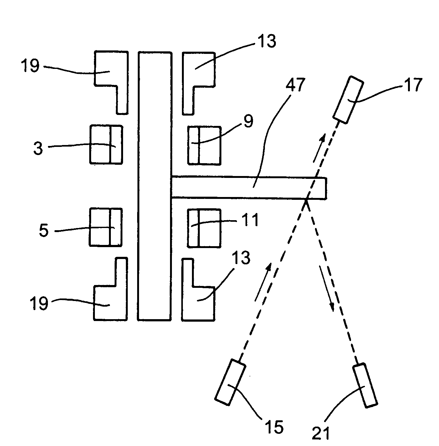
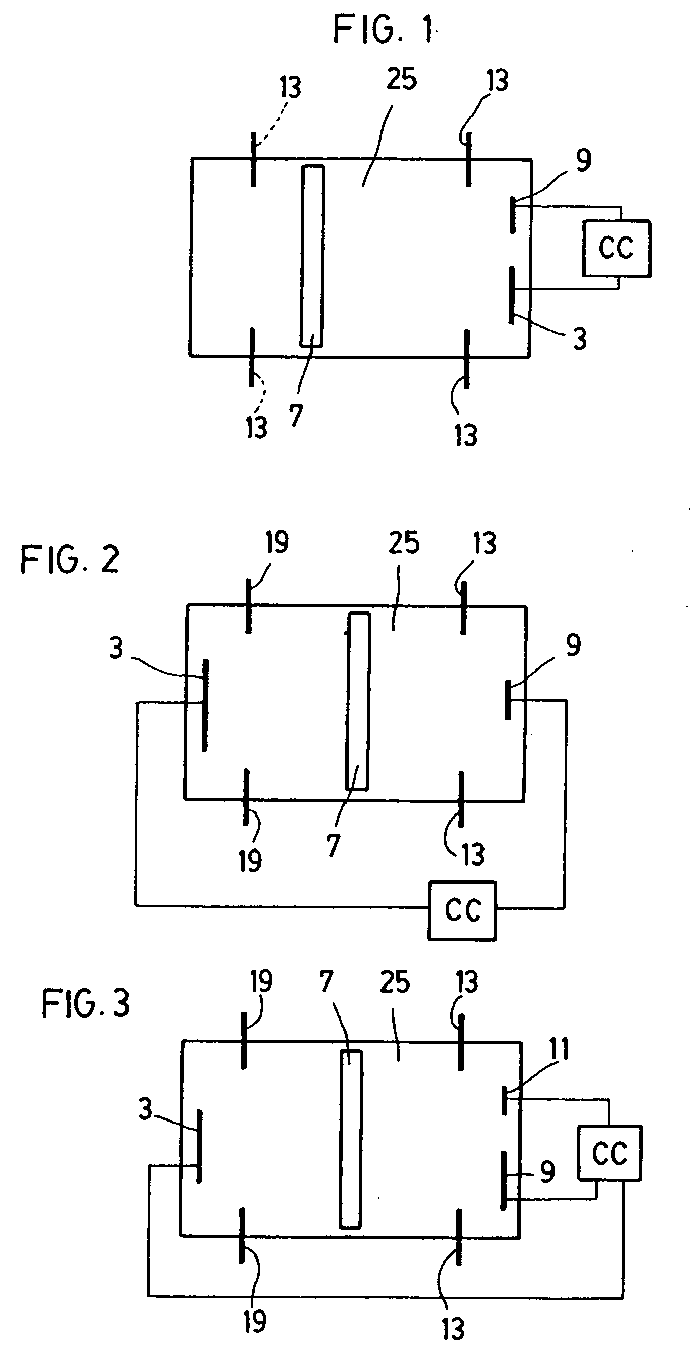
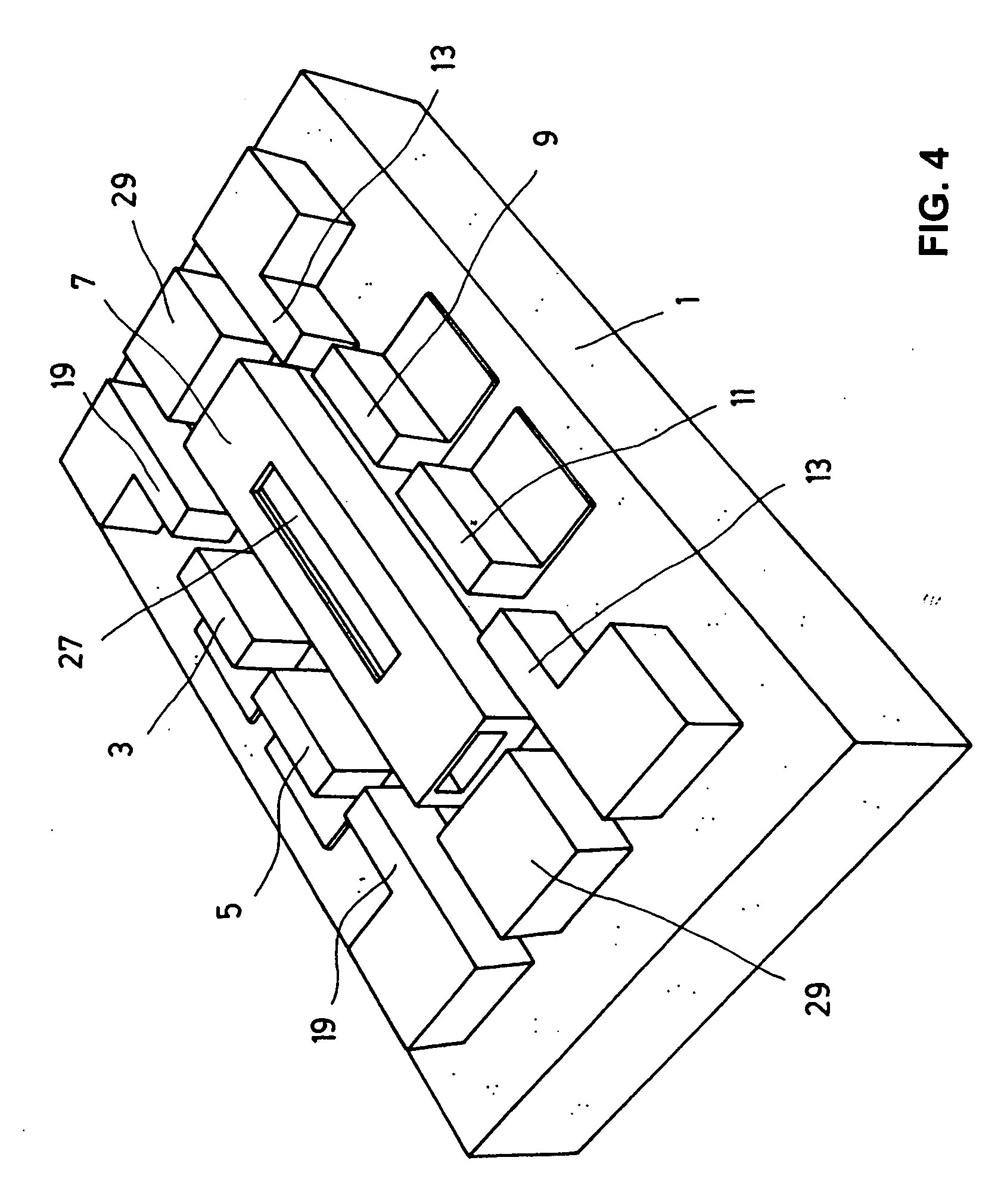
[0075]FIG. 1 shows a first basic functioning mode of an electro-optical device according to the invention. The electro-optical device defines an intermediate space 25 in which is housed a conductive element 7, which can move freely along the intermediate space 25, since physically it is a loose part which is not physically joined to the walls which define the intermediate space 25. The electro-optical device also defines a first zone, on the left in FIG. 1, and a second zone, on the right in FIG. 1. In the second zone are arranged a first condenser plate 3 and a second condenser plate 9. In the example shown in FIG. 1, both condenser plates 3 and 9 have different surface areas, although they can be equal with respect to one another. The first condenser plate 3 and the second condenser plate 9 are connected to a CC control circuit. On applying a voltage between the first condenser plate 3 and the second condenser plate 9, the conductive element is always attracted towards the right i...


PUM


Abstract

A miniaturized electro-optical device having a first zone facing a second zone, a first condenser plate, a second condenser plate arranged in the second zone and smaller than or equal to the first condenser plate, an intermediate space between both zones, with a conductive element arranged therein and which is independent from the side walls and moves thereacross the space depending on voltages present across both plates, two inlet / outlet points for light of an optical circuit, where the conductive element modifies the state of passage of light between the inlet / outlet points, when it is in contact with the stop. The device can be used, for example, as an accelerometer, a tiltmeter, a Coriolis force detector, a microphone, for acoustic applications, for the manufacture of an optical switching matrix, for the projection of images or as a pressure flowrate, temperature, gas, sensor.

Description

FIELD OF THE INVENTION [0001] This invention relates to a miniaturised electro-optical device. The invention also relates to different uses for miniaturised electro-optical devices according to the invention. STATE OF THE ART [0002] All kinds of electro-optical devices and systems are known, used mainly (but not exclusively) in information transmission technology. [0003] On the other hand, also known is the production of miniaturised electro-optical devices in the context of technologies known as MEMS technology (micro electromechanical systems), Microsystems and / or Micromachines. These miniaturised devices are usually electromechanical devices fulfilling functions similar to electromechanical devices of conventional size, such as for example, relays, various types of sensors, pumps, etc. The object of the invention is to provide electro-optical type miniaturised devices, namely, those in which starting out from an electrical signal it is possible to interact in an optical signal. [...

Claims


Application Information

Patent Timeline
Patent Type & Authority Applications(United States)
IPC IPC(8): G01B11/14G01C19/56G01P15/093G01P15/13H01H35/02H01H35/14H01H35/24H01H36/00H01H59/00H01Q3/12H01Q21/06
CPCG01C19/5726G01C19/5755G01P15/093G01P15/131H01H35/02H01H35/14H01H35/24H01H36/00H01H59/0009H01H2036/0093H01H2037/008G02F1/29G02F1/21
Inventor SILVESTRE, JOSEP MONTANYA
Owner BAOLAB MICROSYST
Why Eureka
Try Eureka