Apparatus including 4-way valve for fabricating semiconductor device, method of controlling valve, and method of fabricating semiconductor device using the apparatus

a technology of apparatus and semiconductor, applied in the direction of transportation and packaging, chemical vapor deposition coating, coating, etc., can solve the problems of slow deposition of ald, dead volume (dv), and inability to purge, so as to increase the purge efficiency

Inactive Publication Date: 2006-07-20
SAMSUNG ELECTRONICS CO LTD +1
View PDF16 Cites 23 Cited by
  • Summary
  • Abstract
  • Description
  • Claims
  • Application Information

AI Technical Summary

Benefits of technology

[0030] The present invention provides an apparatus for fabricating a semiconductor device, by which purge efficiency is increased by preventing dead volume from occurring in a gas valve system.

Problems solved by technology

Despite a disadvantage that the ALD is slow in deposition since the chemical reaction is limited to only the surface of a wafer, ALD is essential to fabrication of a dielectric layer, a diffusion preventing layer, a gate dielectric layer, etc., for a memory capacitor that requires a high-purity and high-uniformity thin film.
However, the conventional ALD apparatus has a problem in that dead volume (DV), in which purging is not performed and a source gas material is stagnant between valves, occurs.
In particular, when a dielectric layer or a complex layer, which includes multiple layers made of different materials, is formed using the conventional ALD apparatus, different source gas materials may react with each other in the DV portion, thereby generating unnecessary particles.
As a result, a thin film formed through the ALD may have defects or low uniformity.
Taking into account that an ALD cycle takes several seconds, it is very difficult to perform ALD using different kinds of source gas without purging and removing the source gas remaining in the DV portion.

Method used


Image

  • Apparatus including 4-way valve for fabricating semiconductor device, method of controlling valve, and method of fabricating semiconductor device using the apparatus
  • Apparatus including 4-way valve for fabricating semiconductor device, method of controlling valve, and method of fabricating semiconductor device using the apparatus
  • Apparatus including 4-way valve for fabricating semiconductor device, method of controlling valve, and method of fabricating semiconductor device using the apparatus

Examples


first embodiment

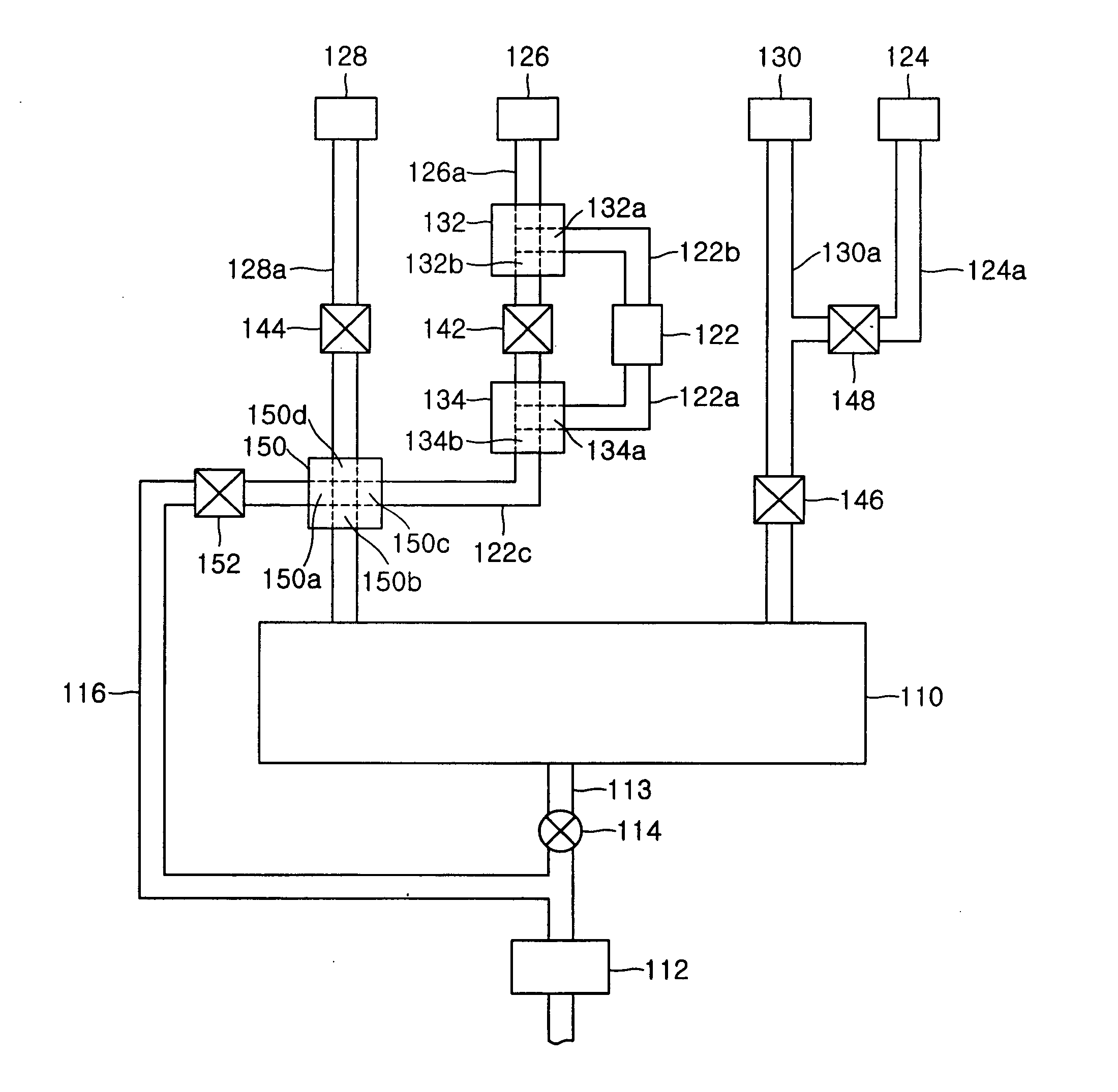
[0058]FIG. 5 is a schematic diagram illustrating an apparatus for fabricating a semiconductor device according to the present invention. FIG. 6 is an enlarged view of a part of the apparatus illustrated in FIG. 5. FIG. 7 is a cross sectional view of the part shown in FIG. 6, taken along the line CC′, in which a 2-way valve is closed. FIG. 8 is a cross sectional view of the part shown in FIG. 6, taken along the line DD′, in which a 4-way valve is closed.

[0059] The apparatus for fabricating a semiconductor device, a valve control method, and a method of fabricating a semiconductor device using the apparatus, according to the first embodiment of the present invention will be described in detail with reference to FIGS. 5 through 8.

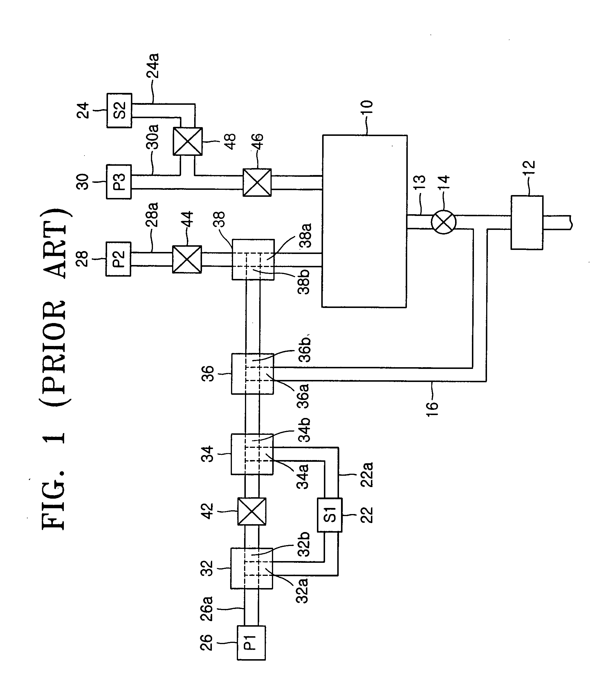
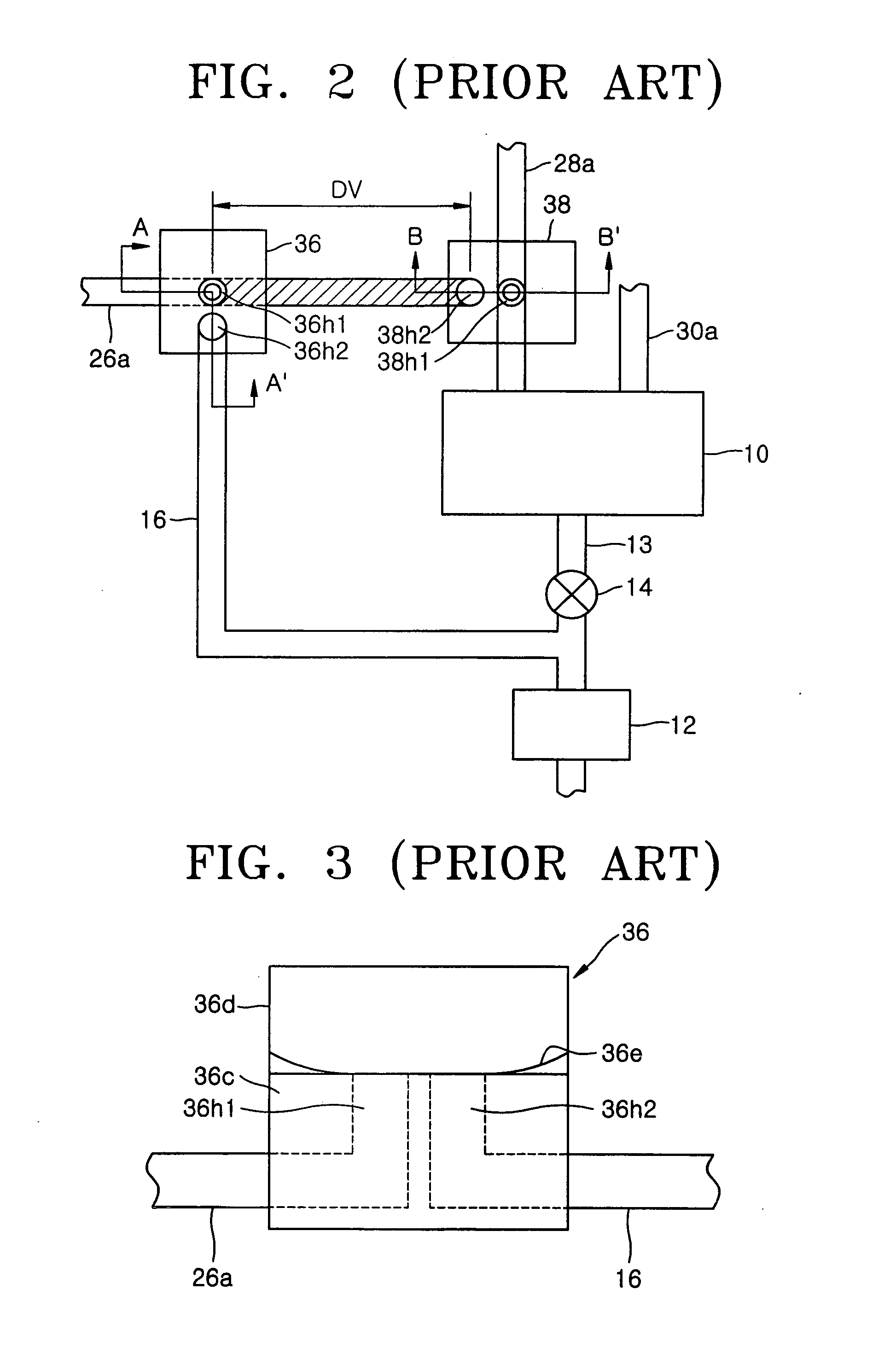
[0060] Referring to FIG. 5, a source gas supply source 122, a reactive gas supply source 124, a purge gas supply source 128, a first carrier gas supply source 126, and a second carrier gas supply source 130 supply a source gas, a reactive gas, a purge gas, an...

third embodiment

[0087] Referring to FIG. 12, each of two source gas supply sources 122 and 222 is installed together with the first carrier gas supply line to be parallel with the source gas supply pipe 122c and the two source gas supply sources 122 and 222 are disposed symmetrically. The apparatus illustrated in FIG. 12 is designed such that one of a first source gas and a second source gas is selectively supplied using a plurality of 2-way gate valves and 3-way valves. In the third embodiment, two kinds of source gas are supplied, but more than two kinds of source gas may be selectively supplied by disposing more than two source supply lines in parallel with the source gas supply pipe 122c.

[0088] In a first source gas supply line starting from the first source gas supply source 122 supplying the first source gas, the carrier gas is supplied from the first carrier gas supply source 126 through the first carrier gas supply pipe 126a to which the first source gas supply source 122 is connected in p...

fourth embodiment

[0101] In a purge gas supply line, the purge gas is supplied from the purge gas supply source 128 to the reaction chamber 110 through the purge gas supply pipe 128a. The first 4-way valve 150 is installed at a junction of the purge gas supply pipe 128a and the first source gas supply pipe 122c. The second 4-way valve 250 is installed at a junction of the purge gas supply pipe 128a and the second source gas supply pipe 222c. The second gate valve 144 is installed between the purge gas supply source 128 and the second 4-way valve 250. In addition, gate valves 152 and 252 are installed at the bypass 116 connected with the first and second 4-way valves 150 and 250. A reactive gas supply line in the fourth embodiment is the same as those in the above-described embodiments.

[0102] The following describes in detail a process of depositing a reaction product of the source gas and the reactive gas on a surface of a substrate through ALD using the first and second source gases A1 and A2 and th...


PUM

PropertyMeasurementUnit
angleaaaaaaaaaa
right angleaaaaaaaaaa
areaaaaaaaaaaa

Abstract

An apparatus and method for fabricating a semiconductor device using a 4-way valve with improved purge efficiency by improving a gas valve system by preventing dead volume from occurring are provided. The apparatus includes a reaction chamber in which a substrate is processed to fabricate a semiconductor device; a first processing gas supply pipe supplying a first processing gas into the reaction chamber; a 4-way valve having a first inlet, a second inlet, a first outlet, and a second outlet and installed at the first processing gas supply pipe such that the first inlet and the first outlet are connected to the first processing gas supply pipe; a second processing gas supply pipe connected to the second inlet of the 4-way valve to supply a second processing gas; a bypass connected to the second outlet of the 4-way valve; and a gate valve installed at the bypass.

Description

CROSS-REFERENCE TO RELATED PATENT APPLICATIONS [0001] This application claims the benefit of Korean Patent Application No. 10-2005-0005074, filed on Jan. 19, 2005, and Korean Patent Application No. 10-2005-0076968, filed on Aug. 22, 2005, in the Korean Intellectual Property Office, the contents of which are incorporated herein in their entirety by reference. BACKGROUND OF THE INVENTION [0002] 1. Field of the Invention [0003] The present invention relates to an apparatus for fabricating a semiconductor device, and more particularly, to an apparatus for fabricating a semiconductor device using a 4-way valve with improved purge efficiency by improving a valve system for gas supplied to a reaction chamber, a method of controlling the 4-way valve, and a method of fabricating a semiconductor device using the apparatus. [0004] 2. Description of the Related Art [0005] Semiconductor devices are fabricated by repeatedly performing processes such as deposition and patterning of a thin layer on...

Claims


Application Information

Patent Timeline
Patent Type & Authority Applications(United States)
IPC IPC(8): C23C16/00C03C25/68H01L21/306H01L21/302H01L21/31
CPCC23C16/45544H01L21/00H01L21/0262C23C16/45561C23C16/0272C23C16/403C23C16/405C23C16/4402C23C16/45574H01L21/02178H01L21/02181H01L21/0228H01L21/28556H01L21/28562Y10T137/0318
Inventor WON, SEOK-JUNYOO, YONG-MINKIM, DAE-YOUNKIM, YOUNG-HOONKWON, DAE-JINKIM, WEON-HONG
Owner SAMSUNG ELECTRONICS CO LTD
Why Eureka
Try Eureka