Memory cell

Inactive Publication Date: 2006-07-20
MACRONIX INT CO LTD
View PDF7 Cites 9 Cited by
  • Summary
  • Abstract
  • Description
  • Claims
  • Application Information

AI Technical Summary

Benefits of technology

[0010] In view of the above, the present invention is directed to provide a memory cell suitable of solving the problems of electricity leakage, increasing the integration of the memory cell, and increasing the efficiency of programming / erasing operations of the memory cell.
[0011] The present invention is also directed to provide a memory cell suitable of enhancing quality of the inter-gate dielectric layer, increasing gate coupling rate of the memory cell, so as to lower the operation voltage, and increase the efficiency, stability and reliability of the memory cell.
[0016] In the present invention, materials with high dielectric constants, such as aluminum-hafnium oxide, are used for fabricating the tunneling dielectric layer. These materials are suitable to form thin films with uniform thickness and good interface properties. These materials also have high thermal stability, and can be used to fabricate integrated circuits with higher integration. Thus, the use of such materials with high dielectric constants can reduce the chance of electricity leakage, and increase the efficiency of programming / erasing operations.
[0017] In addition, other materials, such as aluminum oxide, are used for forming the inter-gate dielectric layer to improve the quality of the inter-gate dielectric layer, increase gate-coupling efficiency of the memory cell, lower operating voltage, and further, increase efficiency of the memory cell.
[0018] Furthermore, the materials used for fabricating the charge trapping layer, the inter-gate dielectric layer and the metal gate layer have high etching selectivity with respect to the insulator, so as to avoid problems of silicon channel erosion during an etching process for the insulator.

Problems solved by technology

There exist, however, certain difficulties to fabricate a thin tunneling oxide layer.
During a process of fabricating a thin tunneling oxide layer, for example, it is difficult to control the uniformity of the thickness and to lower density of defects.
Furthermore, if the tunneling oxide layer is too thin, electric leakage will often occur, which may lower efficiency of data storing processes and reliability of the memory cell.
The use of the foregoing two types of materials in combination will usually cause gate depletion, and, as a result, a barrier will be formed on the interface of the two materials to adversely affect current transfer.
As a result, stability and reliability the memory cell will be lowered.
Furthermore, in an etching process for forming the insulator 113 of the foregoing conventional memory cell, the silicon channel will be easily eroded because of similar etching selectivity of the ONO structure and the insulator.

Method used


Image

  • Memory cell
  • Memory cell

Examples


Embodiment Construction

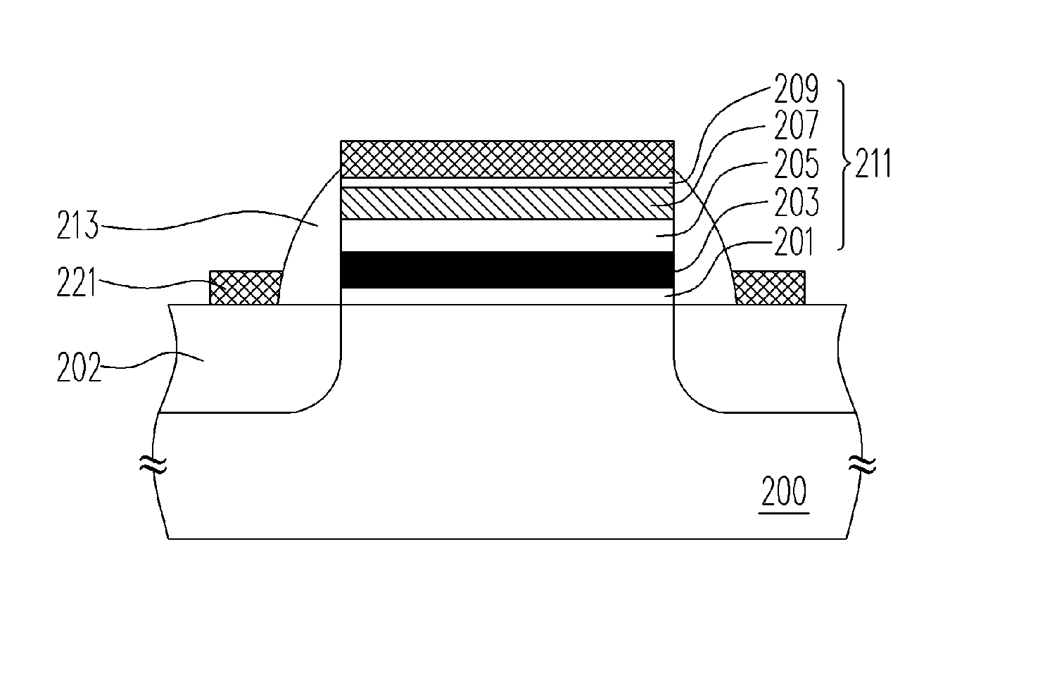
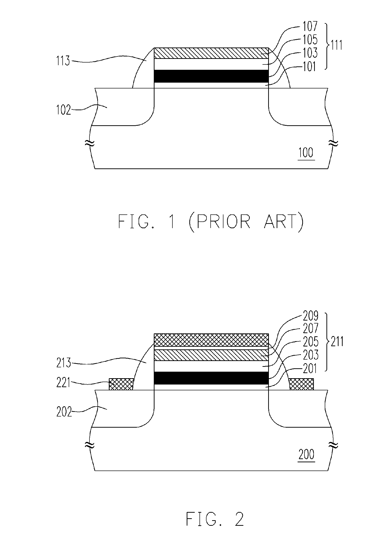
[0022]FIG. 2 shows schematically a structure of a memory cell according to a preferred embodiment of the present invention. As shown in FIG. 2, the memory cell of this invention includes a substrate 200, a gate structure 211, and a source / drain region 202. Wherein, the gate structure 211 is formed on the substrate and the source / drain region 202 is formed in the substrate 200 besides the gate structure 211.

[0023] The gate structure 211 contains, stacking sequentially from the bottom, a tunneling dielectric layer 201, a charge trapping layer 203, an inter-gate dielectric layer 205, and a metal gate layer 207. The tunneling dielectric layer 201 is formed on the substrate 100, the charge trapping layer 203 is formed on the tunneling dielectric layer 201, the inter-gate dielectric layer 205 is form on the charge trapping layer 203, and the metal layer 207 is formed on the inter-gate dielectric layer 205.

[0024] Wherein, the tunneling dielectric layer 201 is made of, for example, alumin...


PUM


Abstract

A memory cell is provided as including a substrate, a tunneling dielectric layer, a charge trapping layer, an inter-gate dielectric layer, a metal gate layer, and a source / drain region. The source / drain region is formed in the substrate besides the gate structure that includes the tunneling dielectric layer, charge trapping layer, inter-gate dielectric layer, and metal gate layer. The tunneling dielectric layer is formed on the substrate, the charge trapping layer is formed on the tunneling dielectric layer, the inter-gate dielectric layer is formed on the charge trapping layer, and the metal gate layer is formed on the inter-gate dielectric layer.

Description

CROSS-REFERENCE TO RELATED APPLICATION [0001] This application claims the priority benefit of Taiwan application serial no. 94101630, filed on Jan. 20, 2005. All disclosure of the Taiwan application is incorporated herein by reference. BACKGROUND OF THE INVENTION [0002] 1. Field of the Invention [0003] The present invention relates to a semiconductor device, and more particularly to a memory cell. [0004] 2. Description of the Related Art [0005] Nonvolatile memory is used today on different electronic devices for purposes of, such as, storing structural data, programming data and other types of data suitable for repeated operations of writing and read. Electrically erasable programmable read only memory (EEPROM) is a type of nonvolatile memory that allows multiple operations of data writing, read and erasing and, furthermore, the data stored therein will not be vanished even after power supply for the memory is cut off. EEPROM hence has been widely used on personal computers and othe...

Claims


Application Information

Patent Timeline
IPC IPC(8): H01L29/788
CPCH01L21/28282H01L29/66833H01L29/792H01L29/40117
Inventor CHANG, KENT KUOHUA
Owner MACRONIX INT CO LTD
Why Eureka
Try Eureka