Efuse structure

a technology of fuses and fuses, applied in the direction of electrical apparatus, semiconductor devices, semiconductor/solid-state device details, etc., can solve the problems of defective circuits, fuses can be selectively blown for repairing, and the whole chip will be unusable, so as to increase the repair yield and the effect of easy blown

Inactive Publication Date: 2006-07-20
UNITED MICROELECTRONICS CORP
View PDF3 Cites 23 Cited by
  • Summary
  • Abstract
  • Description
  • Claims
  • Application Information

AI Technical Summary

Benefits of technology

[0014] Because of the thinner poly silicide layer according to the present invention, the eFuse structure is blown easily to solve the past problem of being hard to control, thereby increasing the repair yield. Furthermo

Problems solved by technology

If a single metal link, a diode, or a MOS is broken down, the whole chip will be unusable.
When defects are found in the circuit, fuses can be selectively blown for repairing or replacing defective circuits.
However, the way of controlling an eFuse to open using electro-migration in the prior art is very difficult and suffers from a low repair yield.
When voltage is too high, the

Method used


Image

  • Efuse structure
  • Efuse structure
  • Efuse structure

Examples


Embodiment Construction

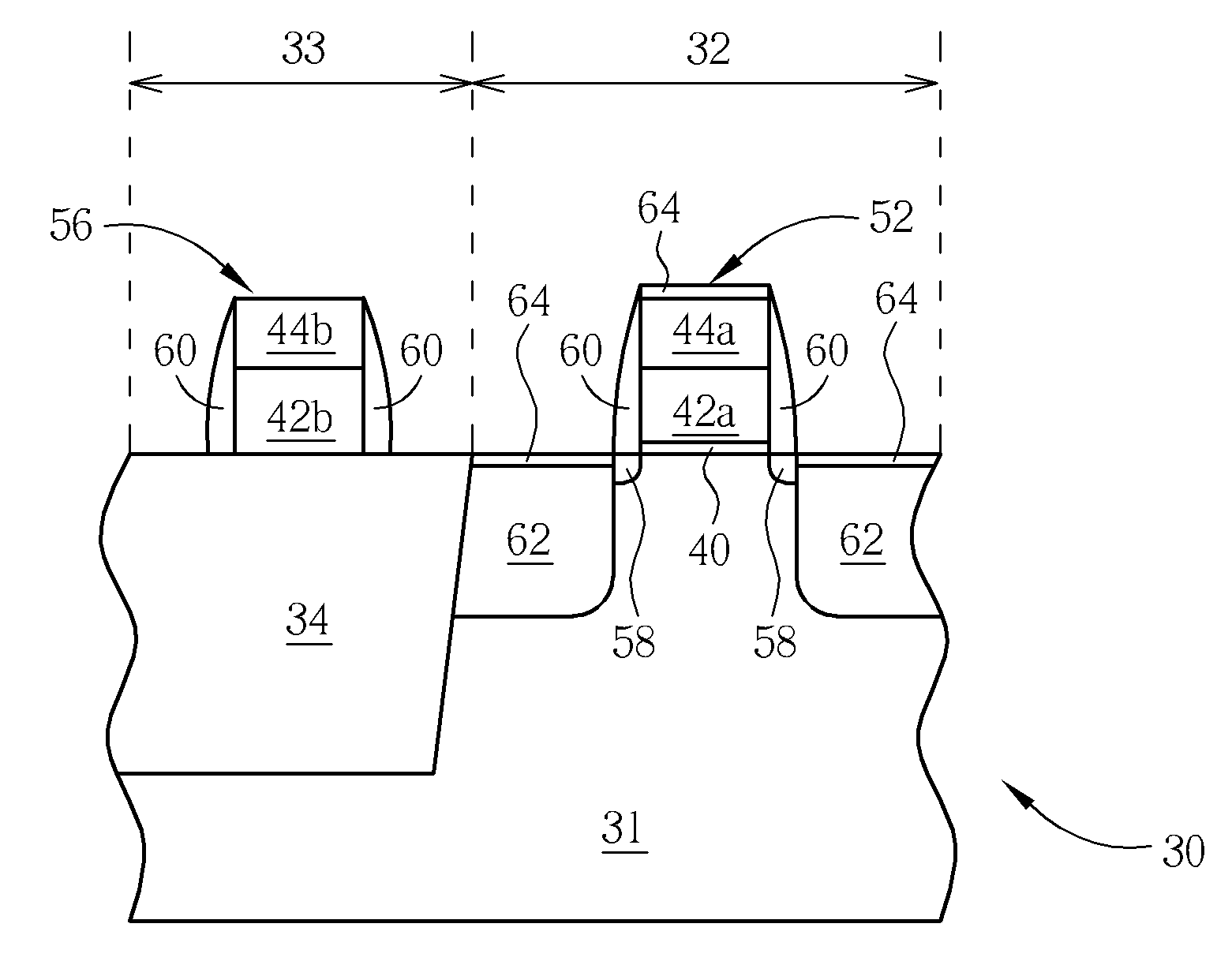
[0020] Please refer to FIGS. 3 to 7. FIGS. 3 to 7 are diagrams of the manufacturing process of an eFuse structure on a semiconductor chip according to the present invention. As shown in FIG. 3, a semiconductor chip 30 comprises a substrate 31 and surface of the substrate 31 includes a first region 32 and a second region 33. The second region 33 forms a plurality of insulting layers called STI (shallow trench isolation) layers or field oxide layers by utilizing a shallow trench isolation process or local oxidation (LOCOS) to surround and isolate the first region 32. The first region 32 forms an active area for a MOS.

[0021]FIG. 4 illustrates a thermal oxidation or CVD (chemical vapor deposition) process used to form silicon dioxide or silicon nitride as a gate insulating layer 40. The depth of the gate insulating layer 40 is almost matched with the surface of the STI (shallow trench isolation) 34. The deposition process forms a poly silicon layer 42 and a poly silicide layer 44. The ...


PUM


Abstract

A surface of a semiconductor substrate comprises at least one electrical conduction structure and at least one eFuse. The electrical conduction structure comprises a first poly silicon layer and a first poly silicide layer formed in the first poly silicon layer. The eFuse comprises a second poly silicon layer and a second poly silicide layer formed on the second poly silicon layer. The area of the second poly silicide layer is smaller than the area of the first poly silicide layer.

Description

BACKGROUND OF INVENTION [0001] 1. Field of the Invention [0002] The invention relates to a structure of an eFuse, and more particularly, to an eFuse structure in which the poly silicide layer is smaller than the poly silicide layer of a gate structure. [0003] 2. Description of the Prior Art [0004] As semiconductor processes become smaller and more complex, semiconductor components are influenced by impurities more easily. If a single metal link, a diode, or a MOS is broken down, the whole chip will be unusable. To treat this problem, fuses can be selectively blown for increasing the yield of IC manufacturing. [0005] In general, fused circuits are redundant circuits of an IC. When defects are found in the circuit, fuses can be selectively blown for repairing or replacing defective circuits. For example, with memory, the top surface of the memory has fuse structures. When the memory cell, word line, or wire contains defects, fuses can be connected with other redundant memory cells, wo...

Claims


Application Information

Patent Timeline
IPC IPC(8): H01L29/00
CPCH01L21/28052H01L23/5256H01L29/665H01L29/7833H01L2924/0002H01L2924/00
Inventor WU, BING-CHANG
Owner UNITED MICROELECTRONICS CORP
Why Eureka
Try Eureka